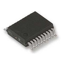
ATA5743P6-TKQY 19 Atmel, ATA5743P6-TKQY 19 Datasheet - Page 13

ATA5743P6-TKQY 19
Manufacturer Part Number
ATA5743P6-TKQY 19
Description
RF Receiver UHF ASK / FSK Receiver
Manufacturer
Atmel
Type
Receiverr
Datasheet
1.ATA5743P3-TGQY.pdf
(43 pages)
Specifications of ATA5743P6-TKQY 19
Package / Case
SSO-20
Operating Frequency
449 MHz
Operating Supply Voltage
4.5 V to 5.5 V
Maximum Operating Temperature
+ 105 C
Minimum Operating Temperature
- 40 C
Mounting Style
SMD/SMT
Noise Figure
7 dB
Lead Free Status / RoHS Status
Lead free / RoHS Compliant
Figure 6-2.
4839B–RKE–08/05
NO
Polling Mode Flow Chart
Sleep Mode:
All circuits for signal processing are
disabled. Only XTO and polling logic are
enabled.
Output level on pin IC_ACTIVE => low
I
T
Start-up Mode:
The signal processing circuits are
enabled. After the start-up time (T
circuits are in a stable condition and ready
to receive.
Output level on pin IC_ACTIVE => high
I
T
Bit-check Mode:
The incoming data stream is analyzed. If
the timing indicates a valid transmitter
signal, the receiver is set to receive mode.
Otherwise it is set to Sleep mode.
Output level on pin IC_ACTIVE => high
I
T
Receiving Mode:
The receiver is turned on permanently
and passes the data stream to the
connected microcontroller. It can be set to
Sleep mode through an OFF command
via pin DATA or POLLING/_ON.
Output level on pin IC_ACTIVE => high
I
S
S
S
S
Sleep
Startup
Bit-check
= I
= I
= I
= I
Soff
Son
Son
Son
= Sleep
OFF command
Bit-check
X
OK?
Sleep
YES
1024
T
Clk
Startup
) all
Sleep:
X
T
T
T
Sleep
Clk
Startup
Bit-check
:
:
:
:
5-bit word defined by Sleep0 to Sleep4 in
OPMODE register
Extension factor defined by X
according to Table 9
Basic clock cycle defined by f
MODE
Defined by the selected baud rate range
and T
by Baud0 and Baud1 in the OPMODE
register
Depends on the result of the bit check
If the bit check is ok, T
on the number of bits to be checked
(N
If the bit check fails, the average time
period for that check depends on the
selected baud-rate range on T
baud-rate range is defined by Baud0 and
Baud1 in the OPMODE register
Bit-check
Clk
. The baud-rate range is defined
), and on the utilized data rate
Bit-check
depends
SleepStd
XTO
Clk
. The
and pin
ATA5743
13


