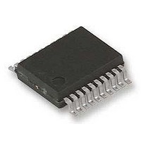
ATA5743P6-TKQY 19 Atmel, ATA5743P6-TKQY 19 Datasheet - Page 11

ATA5743P6-TKQY 19
Manufacturer Part Number
ATA5743P6-TKQY 19
Description
RF Receiver UHF ASK / FSK Receiver
Manufacturer
Atmel
Type
Receiverr
Datasheet
1.ATA5743P3-TGQY.pdf
(43 pages)
Specifications of ATA5743P6-TKQY 19
Package / Case
SSO-20
Operating Frequency
449 MHz
Operating Supply Voltage
4.5 V to 5.5 V
Maximum Operating Temperature
+ 105 C
Minimum Operating Temperature
- 40 C
Mounting Style
SMD/SMT
Noise Figure
7 dB
Lead Free Status / RoHS Status
Lead free / RoHS Compliant
6.1
4839B–RKE–08/05
Basic Clock Cycle of the Digital Circuitry
The complete timing of the digital circuitry and the analog filtering is derived from one clock. As
seen in
tion with a divider. The division factor is controlled by the logical state at pin MODE. As
described in section
defined by the RF input signal (f
oscillator (f
Figure 6-1.
Pin MODE can now be set in accordance with the desired clock cycle T
following application relevant parameters:
Most applications are dominated by two transmission frequencies: f
used in the USA, f
parameters on these electrical characteristics, here are displayed the three conditions for each
parameter.
The clock cycle of some function blocks depends on the selected baud-rate range (BR_Range)
which is defined in the OPMODE register. This clock cycle T
mulas for further reference:
BR_Range =
• Timing of the polling circuit including bit check
• Timing of the analog and digital signal processing
• Timing of the register programming
• Frequency of the reset marker
• IF filter center frequency (f
• Application USA (f
• Application Europe (f
• Other applications (T
electrical characteristic is given as a function of T
Figure
LO
).
Generation of the Basic Clock Cycle
6-1, this clock cycle T
Send
“RF Front-end” on page
XTO
= 433.92 MHz in Europe. In order to ease the usage of all T
XTO
Clk
= 4.90625 MHz, MODE = L, T
is dependent on f
= 6.76438 MHz, MODE = H, T
IF0
BR_Range0:
BR_Range1:
BR_Range2:
BR_Range3:
)
Divider
:14/:10
RFin
XTO
T
f
CLK
) which also defines the operating frequency of the local
XTO
Clk
is derived from the crystal oscillator (XTO) in combina-
XTO
16
15
14
MODE
DVCC
XTO
5, the frequency of the crystal oscillator (f
and on the logical state of pin MODE. The
Clk
L : USA(:10)
H: Europe(:14)
).
T
T
T
T
Clk
XClk
XClk
XClk
XClk
= 2.0383 µs)
Clk
= 8
= 4
= 2
= 1
= 2.0697 µs)
XClk
is defined by the following for-
T
T
T
T
Clk
Clk
Clk
Clk
Send
Clk
= 315 MHz is mainly
, which controls the
ATA5743
Clk
-dependent
XTO
) is
11


