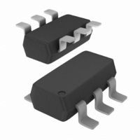
PBLS6003D,115 NXP Semiconductors, PBLS6003D,115 Datasheet - Page 3

PBLS6003D,115
Manufacturer Part Number
PBLS6003D,115
Description
LOADSWITCH PNP 60V 1A SOT457
Manufacturer
NXP Semiconductors
Series
-r
Datasheet
1.PBLS6003D115.pdf
(16 pages)
Specifications of PBLS6003D,115
Package / Case
SC-74-6
Transistor Type
1 NPN Pre-Biased, 1 PNP
Current - Collector (ic) (max)
100mA, 700mA
Voltage - Collector Emitter Breakdown (max)
50V, 60V
Resistor - Base (r1) (ohms)
10K
Resistor - Emitter Base (r2) (ohms)
10K
Dc Current Gain (hfe) (min) @ Ic, Vce
30 @ 5mA, 5V / 150 @ 500mA, 5V
Vce Saturation (max) @ Ib, Ic
150mV @ 500µA, 10mA / 340mV @ 100mA, 1A
Current - Collector Cutoff (max)
1µA, 100nA
Frequency - Transition
185MHz
Power - Max
600mW
Mounting Type
Surface Mount
Configuration
Dual
Transistor Polarity
NPN/PNP
Typical Input Resistor
10 KOhm @ NPN
Typical Resistor Ratio
1 @ NPN
Mounting Style
SMD/SMT
Collector- Emitter Voltage Vceo Max
50 V @ NPN or 60 V @ PNP
Peak Dc Collector Current
100 mA @ NPN or 1000 mA @ PNP
Maximum Operating Temperature
+ 150 C
Minimum Operating Temperature
- 65 C
Lead Free Status / RoHS Status
Lead free / RoHS Compliant
Lead Free Status / RoHS Status
Lead free / RoHS Compliant, Lead free / RoHS Compliant
Other names
934059266115
PBLS6003D T/R
PBLS6003D T/R
PBLS6003D T/R
PBLS6003D T/R
NXP Semiconductors
5. Limiting values
PBLS6003D_2
Product data sheet
Table 5.
In accordance with the Absolute Maximum Rating System (IEC 60134).
[1]
[2]
[3]
Symbol
TR1; PNP low V
V
V
V
I
I
I
I
P
TR2; NPN resistor-equipped transistor
V
V
V
V
I
I
P
Per device
P
T
T
T
C
CM
B
BM
O
CM
stg
j
amb
CBO
CEO
EBO
tot
CBO
CEO
EBO
I
tot
tot
Device mounted on an FR4 PCB, single-sided copper, tin-plated and standard footprint.
Device mounted on an FR4 PCB, single-sided copper, tin-plated, mounting pad for collector 1cm
Device mounted on a ceramic PCB, Al
Limiting values
Parameter
collector-base voltage
collector-emitter voltage
emitter-base voltage
collector current (DC)
peak collector current
base current (DC)
peak base current
total power dissipation
collector-base voltage
collector-emitter voltage
emitter-base voltage
input voltage
output current (DC)
peak collector current
total power dissipation
total power dissipation
storage temperature
junction temperature
ambient temperature
positive
negative
CEsat
transistor
Rev. 02 — 7 September 2009
2
O
3
, standard footprint.
Conditions
open emitter
open base
open collector
single pulse;
t
single pulse;
t
T
open emitter
open base
open collector
T
T
p
p
amb
amb
amb
1 ms
1 ms
25 C
25 C
25 C
[1]
[2]
[3]
[1]
[2]
[3]
[1]
[2]
[3]
[1]
[2]
[3]
60 V PNP BISS loadswitch
Min
-
-
-
-
-
-
-
-
-
-
-
-
-
-
-
-
-
-
-
-
-
-
-
-
-
-
65
65
PBLS6003D
© NXP B.V. 2009. All rights reserved.
Max
250
350
400
50
50
10
+40
100
100
200
200
200
400
530
600
+150
150
+150
80
60
5
700
850
1
2
300
1
10
Unit
V
V
V
mA
mA
A
A
mA
A
mW
mW
mW
V
V
V
V
V
mA
mA
mW
mW
mW
mW
mW
mW
2
C
C
C
.
3 of 16


