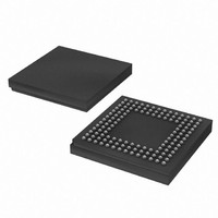
XC3S100E-4CPG132C Xilinx Inc, XC3S100E-4CPG132C Datasheet - Page 36

XC3S100E-4CPG132C
Manufacturer Part Number
XC3S100E-4CPG132C
Description
FPGA Spartan®-3E Family 100K Gates 2160 Cells 572MHz 90nm (CMOS) Technology 1.2V 132-Pin CSBGA
Manufacturer
Xilinx Inc
Series
Spartan™-3Er
Datasheet
1.XC3S100E-4VQG100C.pdf
(233 pages)
Specifications of XC3S100E-4CPG132C
Package
132CSBGA
Family Name
Spartan®-3E
Device Logic Cells
2160
Device Logic Units
240
Device System Gates
100000
Number Of Registers
1920
Maximum Internal Frequency
572 MHz
Typical Operating Supply Voltage
1.2 V
Maximum Number Of User I/os
83
Ram Bits
73728
Number Of Logic Elements/cells
2160
Number Of Labs/clbs
240
Total Ram Bits
73728
Number Of I /o
83
Number Of Gates
100000
Voltage - Supply
1.14 V ~ 1.26 V
Mounting Type
Surface Mount
Operating Temperature
0°C ~ 85°C
Package / Case
132-TFBGA, CSPBGA
Lead Free Status / RoHS Status
Lead free / RoHS Compliant
Other names
122-1515
Available stocks
Company
Part Number
Manufacturer
Quantity
Price
Company:
Part Number:
XC3S100E-4CPG132C
Manufacturer:
Xilinx Inc
Quantity:
10 000
Part Number:
XC3S100E-4CPG132C
Manufacturer:
XILINX/赛灵思
Quantity:
20 000
- Current page: 36 of 233
- Download datasheet (6Mb)
Functional Description
Table 22: Port Aspect Ratios
If the data bus width of Port A differs from that of Port B, the
block RAM automatically performs a bus-matching function
as described in
with a narrow bus and then read from a port with a wide bus,
the latter port effectively combines “narrow” words to form
“wide” words. Similarly, when data is written into a port with
a wide bus and then read from a port with a narrow bus, the
latter port divides “wide” words to form “narrow” words. Par-
36
Notes:
1.
2.
3.
4.
Path Width
Total Data
(w bits)
The width of the total data path (w) is the sum of the DI/DO bus width (w-p) and any parity bits (p).
The width selection made for the DI/DO bus determines the number of address lines (r) according to the relationship expressed as:
r = 14 – [log(w–p)/log(2)].
The number of address lines delimits the total number (n) of addressable locations or depth according to the following equation: n = 2
The product of w and n yields the total block RAM capacity.
18
36
1
2
4
9
DI/DO Data
Bus Width
(w-p bits)
Figure
16
32
1
2
4
8
31. When data is written to a port
1
Parity Bus
DIP/DOP
(p bits)
Width
0
0
0
1
2
4
(r bits)
ADDR
Width
Bus
14
13
12
11
10
9
2
www.xilinx.com
[w-p-1:0]
DI/DO
[15:0]
[31:0]
[0:0]
[1:0]
[3:0]
[7:0]
ity bits are not available if the data port width is configured
as x4, x2, or x1. For example, if a x36 data word (32 data, 4
parity) is addressed as two x18 halfwords (16 data, 2 par-
ity), the parity bits associated with each data byte are
mapped within the block RAM to the appropriate parity bits.
The same effect happens when the x36 data word is
mapped as four x9 words.
DIP/DOP
[p-1:0]
[0:0]
[1:0]
[3:0]
-
-
-
ADDR
[r-1:0]
[13:0]
[12:0]
[11:0]
[10:0]
[9:0]
[8:0]
Locations (n)
Addressable
DS312-2 (v3.8) August 26, 2009
16,384
No. of
8,192
4,096
2,048
1,024
512
Product Specification
3
Block RAM
(w*n bits)
Capacity
16,384
16,384
16,384
18,432
18,432
18,432
r
.
4
R
Related parts for XC3S100E-4CPG132C
Image
Part Number
Description
Manufacturer
Datasheet
Request
R

Part Number:
Description:
IC SPARTAN-3E FPGA 100K 144-TQFP
Manufacturer:
Xilinx Inc
Datasheet:

Part Number:
Description:
IC FPGA SPARTAN-3E 100K 144-TQFP
Manufacturer:
Xilinx Inc
Datasheet:

Part Number:
Description:
FIELD PROGRAMMER
Manufacturer:
Xilinx Inc
Datasheet:

Part Number:
Description:
FPGA Spartan®-3E Family 100K Gates 2160 Cells 572MHz 90nm (CMOS) Technology 1.2V 100-Pin VTQFP
Manufacturer:
Xilinx Inc
Datasheet:

Part Number:
Description:
FPGA Spartan®-3E Family 100K Gates 2160 Cells 572MHz 90nm (CMOS) Technology 1.2V 144-Pin TQFP
Manufacturer:
Xilinx Inc
Datasheet:

Part Number:
Description:
FPGA Spartan®-3E Family 100K Gates 2160 Cells 657MHz 90nm (CMOS) Technology 1.2V 144-Pin TQFP
Manufacturer:
Xilinx Inc
Datasheet:

Part Number:
Description:
Spartan-3E FPGA Family
Manufacturer:
XILINX [Xilinx, Inc]
Datasheet:

Part Number:
Description:
Spartan-3E FPGA Family: Complete Data Sheet
Manufacturer:
XILINX [Xilinx, Inc]
Datasheet:

Part Number:
Description:
IC FPGA SPARTAN-3E 100K 100-VQFP
Manufacturer:
Xilinx Inc
Datasheet:

Part Number:
Description:
IC FPGA SPARTAN-3E 100K 132CSBGA
Manufacturer:
Xilinx Inc
Datasheet:

Part Number:
Description:
IC FPGA SPARTAN-3E 100K 132CSBGA
Manufacturer:
Xilinx Inc
Datasheet:

Part Number:
Description:
IC FPGA SPARTAN-3E 100K 144-TQFP
Manufacturer:
Xilinx Inc
Datasheet:

Part Number:
Description:
IC FPGA SPARTAN 3E 100VQFP
Manufacturer:
Xilinx Inc
Datasheet:

Part Number:
Description:
IC FPGA SPARTAN 3E 144TQFP
Manufacturer:
Xilinx Inc
Datasheet:

Part Number:
Description:
IC CPLD .8K 36MCELL 44-VQFP
Manufacturer:
Xilinx Inc
Datasheet:


