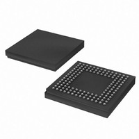
XC3S100E-4CPG132C Xilinx Inc, XC3S100E-4CPG132C Datasheet - Page 125

XC3S100E-4CPG132C
Manufacturer Part Number
XC3S100E-4CPG132C
Description
FPGA Spartan®-3E Family 100K Gates 2160 Cells 572MHz 90nm (CMOS) Technology 1.2V 132-Pin CSBGA
Manufacturer
Xilinx Inc
Series
Spartan™-3Er
Datasheet
1.XC3S100E-4VQG100C.pdf
(233 pages)
Specifications of XC3S100E-4CPG132C
Package
132CSBGA
Family Name
Spartan®-3E
Device Logic Cells
2160
Device Logic Units
240
Device System Gates
100000
Number Of Registers
1920
Maximum Internal Frequency
572 MHz
Typical Operating Supply Voltage
1.2 V
Maximum Number Of User I/os
83
Ram Bits
73728
Number Of Logic Elements/cells
2160
Number Of Labs/clbs
240
Total Ram Bits
73728
Number Of I /o
83
Number Of Gates
100000
Voltage - Supply
1.14 V ~ 1.26 V
Mounting Type
Surface Mount
Operating Temperature
0°C ~ 85°C
Package / Case
132-TFBGA, CSPBGA
Lead Free Status / RoHS Status
Lead free / RoHS Compliant
Other names
122-1515
Available stocks
Company
Part Number
Manufacturer
Quantity
Price
Company:
Part Number:
XC3S100E-4CPG132C
Manufacturer:
Xilinx Inc
Quantity:
10 000
Part Number:
XC3S100E-4CPG132C
Manufacturer:
XILINX/赛灵思
Quantity:
20 000
- Current page: 125 of 233
- Download datasheet (6Mb)
Table 83: DC Characteristics of User I/Os Using Differential Signal Standards
DS312-3 (v3.8) August 26, 2009
Product Specification
Notes:
1.
2.
3.
LVDS_25
BLVDS_25
MINI_LVDS_25
RSDS_25
DIFF_HSTL_I_18
DIFF_HSTL_III_18
DIFF_SSTL18_I
DIFF_SSTL2_I
IOSTANDARD
The numbers in this table are based on the conditions set forth in
Output voltage measurements for all differential standards are made with a termination resistor (R
differential signal pair. The exception is for BLVDS, shown in
At any given time, no more than two of the following differential output standards may be assigned to an I/O bank: LVDS_25, RSDS_25,
MINI_LVDS_25
Attribute
R
Figure 72: External Termination Resistors for BLVDS Transmitter and BLVDS Receiver
(mV)
Min
250
250
300
100
–
–
–
–
Internal
GND level
Logic
V
V
(mV)
V
V
Typ
350
350
OUTN
OUTP
CCO
OD
–
–
–
–
–
–
FPGA
Out
= 2.5V
V
(mV)
Max
OCM
V
V
450
450
600
400
V
–
–
–
–
OD
OH
OL
Figure 71: Differential Output Voltages
50%
= Output common mode voltage =
= Output differential voltage =
= Output voltage indicating a High logic level
= Output voltage indicating a Low logic level
165Ω
165Ω
(mV)
Min
1/4th of Bourns
CAT16-LV4F12
–
–
–
–
–
–
–
–
Part Number
ΔV
V
OCM
OD
(mV)
Max
www.xilinx.com
140Ω
50
–
–
–
–
–
–
–
Figure 72
Table 77
1.125
Min
1.0
1.1
(V)
V
Z
Z
–
–
–
–
–
0
0
V
OUTP
V
below.
= 50Ω
= 50Ω
OD
OUTN
and
V
1.20
Typ
(V)
OCM
–
–
–
–
–
–
–
V
Table
1/4th of Bourns
V
CAT16-PT4F4
OUTP
Part Number
OH
N
P
V
100Ω
OUTP
82.
1.375
- V
Max
(V)
1.4
1.4
–
–
–
–
–
OUTN
Differential
I/O Pair Pins
ds312-3_07_041108
2
+ V
V
FPGA
In
CCO
V
OUTN
OL
(mV)
Min
DC and Switching Characteristics
DS312-3_03_021505
–
–
–
–
–
–
–
–
= 2.5V
T
ΔV
) of 100Ω across the N and P pins of the
OCM
(mV)
Max
50
–
–
–
–
–
–
–
V
V
V
V
CCO
CCO
TT
TT
V
Min
(V)
+ 0.475
+ 0.61
OH
–
–
–
–
– 0.4
– 0.4
V
V
TT
TT
Max
V
(V)
0.4
0.4
– 0.475
– 0.61
–
–
–
–
OL
125
Related parts for XC3S100E-4CPG132C
Image
Part Number
Description
Manufacturer
Datasheet
Request
R

Part Number:
Description:
IC SPARTAN-3E FPGA 100K 144-TQFP
Manufacturer:
Xilinx Inc
Datasheet:

Part Number:
Description:
IC FPGA SPARTAN-3E 100K 144-TQFP
Manufacturer:
Xilinx Inc
Datasheet:

Part Number:
Description:
FIELD PROGRAMMER
Manufacturer:
Xilinx Inc
Datasheet:

Part Number:
Description:
FPGA Spartan®-3E Family 100K Gates 2160 Cells 572MHz 90nm (CMOS) Technology 1.2V 100-Pin VTQFP
Manufacturer:
Xilinx Inc
Datasheet:

Part Number:
Description:
FPGA Spartan®-3E Family 100K Gates 2160 Cells 572MHz 90nm (CMOS) Technology 1.2V 144-Pin TQFP
Manufacturer:
Xilinx Inc
Datasheet:

Part Number:
Description:
FPGA Spartan®-3E Family 100K Gates 2160 Cells 657MHz 90nm (CMOS) Technology 1.2V 144-Pin TQFP
Manufacturer:
Xilinx Inc
Datasheet:

Part Number:
Description:
Spartan-3E FPGA Family
Manufacturer:
XILINX [Xilinx, Inc]
Datasheet:

Part Number:
Description:
Spartan-3E FPGA Family: Complete Data Sheet
Manufacturer:
XILINX [Xilinx, Inc]
Datasheet:

Part Number:
Description:
IC FPGA SPARTAN-3E 100K 100-VQFP
Manufacturer:
Xilinx Inc
Datasheet:

Part Number:
Description:
IC FPGA SPARTAN-3E 100K 132CSBGA
Manufacturer:
Xilinx Inc
Datasheet:

Part Number:
Description:
IC FPGA SPARTAN-3E 100K 132CSBGA
Manufacturer:
Xilinx Inc
Datasheet:

Part Number:
Description:
IC FPGA SPARTAN-3E 100K 144-TQFP
Manufacturer:
Xilinx Inc
Datasheet:

Part Number:
Description:
IC FPGA SPARTAN 3E 100VQFP
Manufacturer:
Xilinx Inc
Datasheet:

Part Number:
Description:
IC FPGA SPARTAN 3E 144TQFP
Manufacturer:
Xilinx Inc
Datasheet:

Part Number:
Description:
IC CPLD .8K 36MCELL 44-VQFP
Manufacturer:
Xilinx Inc
Datasheet:


