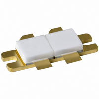
BLF278,112 NXP Semiconductors, BLF278,112 Datasheet - Page 3

BLF278,112
Manufacturer Part Number
BLF278,112
Description
TRANSISTOR RF DMOS SOT262A1
Manufacturer
NXP Semiconductors
Datasheet
1.BLF278112.pdf
(23 pages)
Specifications of BLF278,112
Package / Case
SOT-262A1
Transistor Type
2 N-Channel (Dual)
Frequency
108MHz
Gain
22dB
Voltage - Rated
125V
Current Rating
18A
Current - Test
100mA
Voltage - Test
50V
Power - Output
300W
Minimum Operating Temperature
- 65 C
Mounting Style
SMD/SMT
Resistance Drain-source Rds (on)
0.3 Ohm @ 10 V
Transistor Polarity
N-Channel
Configuration
Dual Common Source
Drain-source Breakdown Voltage
125 V
Gate-source Breakdown Voltage
+/- 20 V
Continuous Drain Current
18 A
Power Dissipation
500000 mW
Maximum Operating Temperature
+ 200 C
Application
VHF
Channel Type
N
Channel Mode
Enhancement
Drain Source Voltage (max)
125V
Power Gain (typ)@vds
20(Min)@50V/18@50V/16@50VdB
Frequency (max)
225MHz
Package Type
CDFM
Pin Count
5
Forward Transconductance (typ)
6.2S
Drain Source Resistance (max)
300@10Vmohm
Input Capacitance (typ)@vds
480@50VpF
Output Capacitance (typ)@vds
190@50VpF
Reverse Capacitance (typ)
14@50VpF
Operating Temp Range
-65C to 200C
Drain Efficiency (typ)
80%
Mounting
Screw
Mode Of Operation
CW Class-AB/CW Class-B/CW Class-C
Number Of Elements
2
Power Dissipation (max)
500000mW
Vswr (max)
7
Screening Level
Military
Lead Free Status / RoHS Status
Lead free / RoHS Compliant
Noise Figure
-
Lead Free Status / Rohs Status
Lead free / RoHS Compliant
Other names
568-2412
933978520112
BLF278
BLF278
933978520112
BLF278
BLF278
Philips Semiconductors
LIMITING VALUES
In accordance with the Absolute Maximum System (IEC 60134).
THERMAL CHARACTERISTICS
2003 Sep 19
handbook, halfpage
Per transistor section
V
V
I
P
T
T
R
R
D
stg
j
DS
GS
tot
th j-mb
th mb-h
VHF push-pull power MOS transistor
Total device; both sections equally loaded.
(1) Current is this area may be limited by R
(2) T
SYMBOL
SYMBOL
(A)
I D
100
10
mb
1
1
= 25 C.
(1)
drain-source voltage
gate-source voltage
drain current (DC)
total power dissipation
storage temperature
junction temperature
thermal resistance from junction
to mounting base
thermal resistance from
mounting base to heatsink
Fig.2 DC SOAR.
10
PARAMETER
PARAMETER
(2)
DSon
100
.
V
DS
MRA988
(V)
500
T
sections equally loaded
total device; both sections
equally loaded.
total device; both sections
equally loaded.
mb
25 C; total device; both
3
CONDITIONS
CONDITIONS
handbook, halfpage
Total device; both sections equally loaded.
(1) Continuous operation.
(2) Short-time operation during mismatch.
P tot
(W)
500
400
300
200
100
0
0
Fig.3 Power derating curves.
40
(1)
65
MIN.
max. 0.35
max. 0.15
80
VALUE
(2)
125
18
500
150
200
Product Specification
20
120
MAX.
T h ( C)
BLF278
MGE616
UNIT
160
K/W
K/W
V
V
A
W
C
C
UNIT


