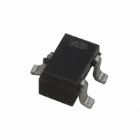
BAP50-05W,115 NXP Semiconductors, BAP50-05W,115 Datasheet - Page 3

BAP50-05W,115
Manufacturer Part Number
BAP50-05W,115
Description
DIODE PIN GP 50V 50MA SOT-323
Manufacturer
NXP Semiconductors
Datasheet
1.BAP50-05W115.pdf
(8 pages)
Specifications of BAP50-05W,115
Package / Case
SC-70-3, SOT-323-3
Diode Type
PIN - 1 Pair Common Cathode
Voltage - Peak Reverse (max)
50V
Current - Max
50mA
Capacitance @ Vr, F
0.5pF @ 5V, 1MHz
Resistance @ If, F
5 Ohm @ 10mA, 100MHz
Power Dissipation (max)
240mW
Configuration
Dual Common Cathode
Reverse Voltage
50 V
Forward Continuous Current
50 mA
Carrier Life
1.05 us
Forward Voltage Drop
1.1 V
Maximum Diode Capacitance
0.5 pF @ 5 V
Maximum Operating Temperature
+ 150 C
Maximum Series Resistance @ Maximum If
5 Ohm @ 10 mA
Maximum Series Resistance @ Minimum If
40 Ohm @ 0.5 mA
Minimum Operating Temperature
- 65 C
Mounting Style
SMD/SMT
Power Dissipation
240 mW
Forward Current
50mA
Forward Voltage
1.1V
Operating Temperature Classification
Military
Package Type
SC-70
Mounting
Surface Mount
Typical Carrier Life Time
1.05us
Operating Temperature (max)
150C
Operating Temperature (min)
-65C
Pin Count
3
Lead Free Status / RoHS Status
Lead free / RoHS Compliant
Lead Free Status / RoHS Status
Lead free / RoHS Compliant, Lead free / RoHS Compliant
Other names
568-1920-2
934056537115
BAP50-05W T/R
934056537115
BAP50-05W T/R
NXP Semiconductors
ELECTRICAL CHARACTERISTICS
T
Note
1. Guaranteed on AQL basis: inspection level S4, AQL 1.0.
THERMAL CHARACTERISTICS
2001 Apr 17
Per diode
V
V
I
C
r
s
s
s
s
L
R
j
SYMBOL
R
SYMBOL
D
L
S
= 25 C unless otherwise specified.
F
R
21
21
21
21
General purpose PIN diode
d
th j-s
2
2
2
2
forward voltage
reverse voltage
reverse current
diode capacitance
diode forward resistance
isolation
insertion loss
insertion loss
insertion loss
charge carrier life time
series inductance
thermal resistance from junction to soldering point
PARAMETER
PARAMETER
I
I
V
V
V
V
I
I
I
V
V
V
I
I
I
I
I
I
I
I
I
when switched from I
I
measured at I
I
F
R
F
F
F
F
F
F
F
F
F
F
F
F
R
F
R
R
R
R
R
R
R
= 50 mA
= 0.5 mA; f = 100 MHz; note 1
= 1 mA; f = 100 MHz; note 1
= 10 mA; f = 100 MHz; note 1
= 0.5 mA; f = 900 MHz
= 0.5 mA; f = 1800 MHz
= 0.5 mA; f = 2450 MHz
= 1 mA; f = 900 MHz
= 1 mA; f = 1800 MHz
= 1 mA; f = 2450 MHz
= 10 mA; f = 900 MHz
= 10 mA; f = 1800 MHz
= 10 mA; f = 2450 MHz
= 100 mA; f = 100 MHz
= 10 A
= 6 mA; R
= 50 V
= 0; f = 1 MHz
= 1 V; f = 1 MHz
= 5 V; f = 1 MHz
= 0; f = 900 MHz
= 0; f = 1800 MHz
= 0; f = 2450 MHz
3
CONDITIONS
L
R
= 100 ;
= 3 mA
F
= 10 mA to
50
MIN.
0.95
0.45
0.35
0.3
25
14
3
19
15.7
13.5
1.84
1.90
1.92
1.08
1.13
1.17
0.26
0.30
0.36
1.05
1.6
TYP.
VALUE
BAP50-05W
250
Product specification
1.1
100
0.6
0.5
40
25
5
MAX.
UNIT
K/W
V
V
nA
pF
pF
pF
dB
dB
dB
dB
dB
dB
dB
dB
dB
dB
dB
dB
s
nH
UNIT


