M3004LD STMicroelectronics, M3004LD Datasheet - Page 3
M3004LD
Manufacturer Part Number
M3004LD
Description
Communication ICs - Various Remote Control Transmitter
Manufacturer
STMicroelectronics
Type
Remote Control Transmitterr
Datasheet
1.M3004LD.pdf
(14 pages)
Specifications of M3004LD
Mounting Style
SMD/SMT
Operating Supply Voltage
2.5 V, 3.3 V, 5 V
Supply Type
Analog
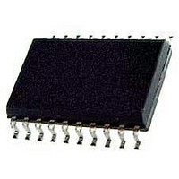
Package / Case
SO-20
Supply Voltage (max)
6.5 V
Supply Voltage (min)
2 V
Supply Current
1 mA
Maximum Operating Temperature
+ 70 C
Minimum Operating Temperature
- 20 C
Operating Supply Voltage (typ)
2.5/3.3/5V
Operating Supply Voltage (min)
2V
Operating Supply Voltage (max)
6.5V
Operating Temp Range
-20C to 70C
Operating Temperature Classification
Commercial
Package Type
SOIC
Mounting
Surface Mount
Pin Count
20
Lead Free Status / RoHS Status
Lead free / RoHS Compliant
Available stocks
Company
Part Number
Manufacturer
Quantity
Price

Part Number:
M3004LD
Manufacturer:
ST
Quantity:
20 000
Company:
Part Number:
M3004LDT
Manufacturer:
SUMIDA
Quantity:
30 000


REMOTE CONTROL SIGNAL OUTPUT (REMO)
The REMO signal output stage is a push-pull type.
In the HIGH state, a bipolar emitter-follower allows
a high output current. The timing of the data output
format is listed in Table 1 and 2. The information is
defined by the distance tb between the leading
edges of the flashed pulses or the first edge of the
modulated pulses (see Figure 6). The format of the
output data is given in Figure 5 and 6. The data
word starts with two toggle bits T1 and T0, fol-
lowed by three bits for defining the sub-system ad-
dress S2, S1 and S0, and six bits F, E, D, C, Band
A which are defined by the selected key.
In the modulated transmission mode the first tog-
gle bit is replaced by a constant reference time bit
(REF). This can be used as a reference time for
the decoding sequence. The toggle bits function is
an indication for the decoder that the next instruc-
tion has to be considered as a new command. The
codes for the sub-system address and the select-
ed key are given in Table 3 and 4.
The REMO output is protected against ”Lock-up”,
i.e. the length of an output pulse is limited to <1ms,
even if the oscillator stops during an output pulse.
This avoids the rapid discharge of the battery that
would otherwise be caused by the continuous ac-
tivation of the LED.
OSCILLATOR INPUT / OUTPUT
(OSCI and OSCO)
The external components must be connected to
these pins when using an oscillator with a ceramic
resonator. The oscillator frequency may vary be-
tween 350kHz and 600kHz as defined by the res-
onator.
FUNCTIONAL DESCRIPTION
Keyboard operation
In the stand-by mode all drivers (DRV0N to
DRV6N) are on (low impedance to V
ever a key is pressed, one or more of the sense in-
puts (SENnN) are tied to ground. This will start the
power-up sequence. First the oscillator is activat-
ed and after the debounce time t
the output drivers (DRV0N to DRV6N) become ac-
tive successively.
Within the first scan cycle the transmission mode,
the applied sub-system address and the selected
command code are sensed and loaded into an in-
ternal data latch.
DB
(see Figure 7)
SS
). When
In contrast to the command code, the sub-system
is sensed only within the first scan cycle. If the ap-
plied sub-system address is changed while the
command key is pressed, the transmitted sub-sys-
tem address is not altered.
In a multiple key stroke sequence (see Figure 8)
the command code is always altered in accor-
dance with the sensed key.
MULTIPLE KEY-STROKE PROTECTION
The keyboard is protected against multiple key-
strokes. If more than one key is pressed at the
same time, the circuit will not generate a new out-
put at REMO (see Figure 8). In case of a multiple
key-stroke, the scan repetition rate is increased to
detect the release of a key as soon as possible.
There are two restrictions caused by the special
structure of the keyboard matrix:
– The keys switching to ground (code numbers 7,
– SEN5N and SEN6N are not protected against
OUTPUT SEQUENCE (data format)
The output operation will start when the selected
code is found. A burst of pulses, including the
latched address and command codes, is generat-
ed at the output REMO as long as a key is
pressed.
The format of the output pulse train is given in Fig-
ure 5 and 6. The operation is terminated by releas-
ing the key or if more than one key is pressed at
the same time. Once a sequence is started, the
transmitted data words will always be completed
after the key is released.
The toggle bits T0 and T1 are incremented if the
key is released for a minimum time t
ure 7). The toggle bits remain unchanged within a
multiple key-stroke sequence.
15, 23, 31, 39, 47, 55 and 63) and the keys
connectedto SEN5N and SEN6N are not
covered completely by the multiple key
protection. If one sense input is switched to
ground,further keys on the same sense line are
ignored, i.e. the command code corresponding
to ”key to ground” is transmitted.
multiple keystroke on the same driver line,
because this condition has been used for the
definition of additional codes (code number 56
to 63).
REL
M3004
(see Fig-
3/14
Related parts for M3004LD
Image
Part Number
Description
Manufacturer
Datasheet
Request
R

Part Number:
Description:
STMicroelectronics [RIPPLE-CARRY BINARY COUNTER/DIVIDERS]
Manufacturer:
STMicroelectronics
Datasheet:
Part Number:
Description:
STMicroelectronics [LIQUID-CRYSTAL DISPLAY DRIVERS]
Manufacturer:
STMicroelectronics
Datasheet:

Part Number:
Description:
BOARD EVAL FOR MEMS SENSORS
Manufacturer:
STMicroelectronics
Datasheet:
Part Number:
Description:
NPN TRANSISTOR POWER MODULE
Manufacturer:
STMicroelectronics
Datasheet:
Part Number:
Description:
TURBOSWITCH ULTRA-FAST HIGH VOLTAGE DIODE
Manufacturer:
STMicroelectronics
Datasheet:
Part Number:
Description:
Manufacturer:
STMicroelectronics
Datasheet:
Part Number:
Description:
DIODE / SCR MODULE
Manufacturer:
STMicroelectronics
Datasheet:
Part Number:
Description:
DIODE / SCR MODULE
Manufacturer:
STMicroelectronics
Datasheet:
Part Number:
Description:
Search -----> STE16N100
Manufacturer:
STMicroelectronics
Datasheet:
Part Number:
Description:
Search ---> STE53NA50
Manufacturer:
STMicroelectronics
Datasheet:
Part Number:
Description:
NPN Transistor Power Module
Manufacturer:
STMicroelectronics
Datasheet:
Part Number:
Description:
DIODE / SCR MODULE
Manufacturer:
STMicroelectronics
Datasheet: