NTHD3100CT1G ON Semiconductor, NTHD3100CT1G Datasheet - Page 4
NTHD3100CT1G
Manufacturer Part Number
NTHD3100CT1G
Description
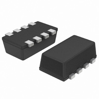
MOSFET N/P-CH 20V 2.9A CHIPFET
Manufacturer
ON Semiconductor
Datasheet
1.NTHD3100CT1G.pdf
(8 pages)
Specifications of NTHD3100CT1G
Fet Type
N and P-Channel
Fet Feature
Logic Level Gate
Rds On (max) @ Id, Vgs
80 mOhm @ 2.9A, 4.5V
Drain To Source Voltage (vdss)
20V
Current - Continuous Drain (id) @ 25° C
2.9A, 3.2A
Vgs(th) (max) @ Id
1.2V @ 250µA
Gate Charge (qg) @ Vgs
2.3nC @ 4.5V
Input Capacitance (ciss) @ Vds
165pF @ 10V
Power - Max
1.1W
Mounting Type
Surface Mount
Package / Case
8-ChipFET™
Configuration
Dual Dual Drain
Transistor Polarity
N and P-Channel
Resistance Drain-source Rds (on)
0.08 Ohm @ 4.5 V
Forward Transconductance Gfs (max / Min)
6 S, 8 S
Drain-source Breakdown Voltage
20 V
Gate-source Breakdown Voltage
+/- 12 V @ N Channel or +/- 8 V @ P Channel
Continuous Drain Current
2.9 A @ N Channel or 3.2 A @ P Channel
Power Dissipation
1100 mW
Maximum Operating Temperature
+ 150 C
Mounting Style
SMD/SMT
Minimum Operating Temperature
- 55 C
Lead Free Status / RoHS Status
Lead free / RoHS Compliant
Other names
NTHD3100CT1GOSTR
Available stocks
Company
Part Number
Manufacturer
Quantity
Price
Company:

Part Number:
NTHD3100CT1G
Manufacturer:
ON
Quantity:
2 400


0.15
0.05
0.1
8
6
4
2
0
0
1.5
1.3
0.9
1.7
1.1
0.7
0
0
Figure 3. On−Resistance vs. Gate−to−Source
−50
V
I
V
1
D
V
DS
GS
Figure 1. On−Region Characteristics
GS
= 2.9 A
2.2 V
−25
, DRAIN−TO−SOURCE VOLTAGE (VOLTS)
Figure 5. On−Resistance Variation with
1
= 4.5 V
, GATE−TO−SOURCE VOLTAGE (VOLTS)
2
V
V
GS
GS
T
J
, JUNCTION TEMPERATURE (°C)
= 5 V to 3 V
= 2.4 V
3
0
2
4
Voltage
25
Temperature
5
3
TYPICAL N−CHANNEL PERFORMANCE CURVES
50
6
1.8 V
1.4 V
1.6 V
2 V
75
4
7
(T
T
I
T
100
D
J
8
J
J
= 2.9 A
= 25°C
= 25°C
= 25°C unless otherwise noted)
5
http://onsemi.com
9
125
10
6
150
4
0.07
0.04
100
0.1
10
1
8
6
4
2
0
2
Figure 4. On−Resistance vs. Drain Current and
1
0
V
GS
Figure 6. Drain−to−Source Leakage Current
V
T
V
V
4
DS
J
= 0 V
DS
GS
= 25°C
0.5
≥ 10 V
Figure 2. Transfer Characteristics
, DRAIN−TO−SOURCE VOLTAGE (VOLTS)
, GATE−TO−SOURCE VOLTAGE (VOLTS)
I
6
D,
DRAIN CURRENT (AMPS)
25°C
3
1
8
T
Gate Voltage
C
V
V
= −55°C
GS
T
vs. Voltage
GS
10
J
= 100°C
= 4.5 V
= 2.5 V
1.5
12
100°C
5
14
2
16
2.5
7
18
20
3
Related parts for NTHD3100CT1G
Image
Part Number
Description
Manufacturer
Datasheet
Request
R

Part Number:
Description:
ON Semiconductor [VOLTAGE REGULATOR]
Manufacturer:
ON Semiconductor
Datasheet:
Part Number:
Description:
357-036-542-201 CARDEDGE 36POS DL .156 BLK LOPRO
Manufacturer:
ON Semiconductor
Datasheet:
Part Number:
Description:
357-036-542-201 CARDEDGE 36POS DL .156 BLK LOPRO
Manufacturer:
ON Semiconductor
Datasheet:
Part Number:
Description:
357-036-542-201 CARDEDGE 36POS DL .156 BLK LOPRO
Manufacturer:
ON Semiconductor
Datasheet:
Part Number:
Description:
357-036-542-201 CARDEDGE 36POS DL .156 BLK LOPRO
Manufacturer:
ON Semiconductor
Datasheet:
Part Number:
Description:
357-036-542-201 CARDEDGE 36POS DL .156 BLK LOPRO
Manufacturer:
ON Semiconductor
Datasheet:
Part Number:
Description:
357-036-542-201 CARDEDGE 36POS DL .156 BLK LOPRO
Manufacturer:
ON Semiconductor
Datasheet:
Part Number:
Description:
357-036-542-201 CARDEDGE 36POS DL .156 BLK LOPRO
Manufacturer:
ON Semiconductor
Datasheet:
Part Number:
Description:
357-036-542-201 CARDEDGE 36POS DL .156 BLK LOPRO
Manufacturer:
ON Semiconductor
Datasheet:
Part Number:
Description:
357-036-542-201 CARDEDGE 36POS DL .156 BLK LOPRO
Manufacturer:
ON Semiconductor
Datasheet:
Part Number:
Description:
357-036-542-201 CARDEDGE 36POS DL .156 BLK LOPRO
Manufacturer:
ON Semiconductor
Datasheet:
Part Number:
Description:
Manufacturer:
ON Semiconductor
Datasheet:
Part Number:
Description:
Manufacturer:
ON Semiconductor
Datasheet:
Part Number:
Description:
Manufacturer:
ON Semiconductor
Datasheet: