NTHD3100CT1G ON Semiconductor, NTHD3100CT1G Datasheet

MOSFET N/P-CH 20V 2.9A CHIPFET

NTHD3100CT1G

Manufacturer Part Number
NTHD3100CT1G
Description
MOSFET N/P-CH 20V 2.9A CHIPFET
Manufacturer
ON Semiconductor
Datasheet

Specifications of NTHD3100CT1G

Fet Type
N and P-Channel
Fet Feature
Logic Level Gate
Rds On (max) @ Id, Vgs
80 mOhm @ 2.9A, 4.5V
Drain To Source Voltage (vdss)
20V
Current - Continuous Drain (id) @ 25° C
2.9A, 3.2A
Vgs(th) (max) @ Id
1.2V @ 250µA
Gate Charge (qg) @ Vgs
2.3nC @ 4.5V
Input Capacitance (ciss) @ Vds
165pF @ 10V
Power - Max
1.1W
Mounting Type
Surface Mount
Package / Case
8-ChipFET™
Configuration
Dual Dual Drain
Transistor Polarity
N and P-Channel
Resistance Drain-source Rds (on)
0.08 Ohm @ 4.5 V
Forward Transconductance Gfs (max / Min)
6 S, 8 S
Drain-source Breakdown Voltage
20 V
Gate-source Breakdown Voltage
+/- 12 V @ N Channel or +/- 8 V @ P Channel
Continuous Drain Current
2.9 A @ N Channel or 3.2 A @ P Channel
Power Dissipation
1100 mW
Maximum Operating Temperature
+ 150 C
Mounting Style
SMD/SMT
Minimum Operating Temperature
- 55 C
Lead Free Status / RoHS Status
Lead free / RoHS Compliant
Other names
NTHD3100CT1GOSTR

Available stocks

Company
Part Number
Manufacturer
Quantity
Price
Part Number:
NTHD3100CT1G
Manufacturer:
ON
Quantity:
2 400
NTHD3100C
Power MOSFET
20 V, +3.9 A /−4.4 A,
Complementary ChipFETt
Features
Applications
Stresses exceeding Maximum Ratings may damage the device. Maximum
Ratings are stress ratings only. Functional operation above the Recommended
Operating Conditions is not implied. Extended exposure to stresses above the
Recommended Operating Conditions may affect device reliability.
1. Surface−mounted on FR4 board using 1 in sq pad size (Cu area = 1.127 in sq
© Semiconductor Components Industries, LLC, 2006
March, 2006 − Rev. 3
MAXIMUM RATINGS
Drain−to−Source Voltage
Gate−to−Source Voltage
N−Channel
P−Channel
Power Dissipation
Pulsed Drain Current
Operating Junction and Storage Temperature
Source Current (Body Diode)
Lead Temperature for Soldering Purposes
Powered Products
Complementary N−Channel and P−Channel MOSFET
Small Size, 40% Smaller than TSOP−6 Package
Leadless SMD Package Provides Great Thermal Characteristics
Trench P−Channel for Low On Resistance
Low Gate Charge N−Channel for Test Switching
Pb−Free Packages are Available
DC−DC Conversion Circuits
Load Switch Applications Requiring Level Shift
Drive Small Brushless DC Motors
Ideal for Power Management Applications in Portable, Battery
[1 oz] including traces).
Continuous Drain
Current (Note 1)
Continuous Drain
Current (Note 1)
(Note 1)
(Note 1)
(1/8″ from case for 10 seconds)
Parameter
(T
J
t ≤ 10 s
t ≤ 10 s
Steady
Steady
Steady
t ≤ 5 s
N−Ch
P−Ch
State
State
State
= 25°C unless otherwise noted)
N−Ch
P−Ch
T
T
T
T
T
T
T
t = 10 ms
t = 10 ms
A
A
A
A
A
A
A
= 25°C
= 25°C
= 25°C
= 85°C
= 25°C
= 85°C
= 25°C
Symbol
V
T
V
I
P
T
STG
T
DSS
DM
I
I
I
GS
D
D
S
J
D
L
,
−55 to
Value
"8.0
"12
−3.2
−2.3
−4.4
−13
150
260
2.9
2.1
3.9
1.1
3.1
2.5
20
12
1
Unit
°C
°C
W
V
V
A
A
A
A
G
See detailed ordering and shipping information in the package
dimensions section on page 7 of this data sheet.
1
N−Channel
P−Channel
V
(BR)DSS
N−Channel MOSFET
−20 V
D
D
D
D
20 V
1
1
2
2
CONNECTIONS
1
C9
M
G
8
7
6
5
ORDERING INFORMATION
D
1
PIN
http://onsemi.com
S
8
64 mW @ −4.5 V
85 mW @ −2.5 V
58 mW @ 4.5 V
77 mW @ 2.5 V
1
= Specific Device Code
= Month Code
= Pb−Free Package
1
2
3
4
R
DS(on)
S
G
S
G
1
2
1
2
Publication Order Number:
G
2
Typ
1
2
3
4
P−Channel MOSFET
CASE 1206A
MARKING
DIAGRAM
ChipFET
STYLE 2
NTHD3100C/D
S 2
AND PIN A
I
D
−4.4 A
3.9 A
D
MAX
2
8
7
6
5

Related parts for NTHD3100CT1G

NTHD3100CT1G Summary of contents

Page 1

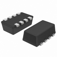
NTHD3100C Power MOSFET 20 V, +3.9 A /−4.4 A, Complementary ChipFETt Features • Complementary N−Channel and P−Channel MOSFET • Small Size, 40% Smaller than TSOP−6 Package • Leadless SMD Package Provides Great Thermal Characteristics • Trench P−Channel for Low On ...

Page 2

THERMAL RESISTANCE RATINGS Parameter Junction−to−Ambient − Steady State (Note 2) Junction−to−Ambient − t ≤ (Note 2) 2. Surface−mounted on FR4 board using pad size (Cu area = 1.127 oz] including traces). ELECTRICAL ...

Page 3

ELECTRICAL CHARACTERISTICS Parameter SWITCHING CHARACTERISTICS (Note 4) Turn−On Delay Time Rise Time Turn−Off Delay Time Fall Time Turn−On Delay Time Rise Time Turn−Off Delay Time Fall Time DRAIN−SOURCE DIODE CHARACTERISTICS Forward Diode Voltage Reverse Recovery Time Charge Time Discharge Time ...

Page 4

TYPICAL N−CHANNEL PERFORMANCE CURVES DRAIN−TO−SOURCE ...

Page 5

TYPICAL N−CHANNEL PERFORMANCE CURVES 400 ISS 300 C RSS 200 100 GATE−TO−SOURCE OR DRAIN−TO−SOURCE VOLTAGE (VOLTS) Figure 7. Capacitance Variation ...

Page 6

TYPICAL P−CHANNEL PERFORMANCE CURVES − −3 − −2 −V , DRAIN−TO−SOURCE VOLTAGE ...

Page 7

... G Figure 19. Resistive Switching Time Variation vs. Gate Resistance DEVICE ORDERING INFORMATION Device NTHD3100CT1 NTHD3100CT1G NTHD3100CT3 NTHD3100CT3G †For information on tape and reel specifications, including part orientation and tape sizes, please refer to our Tape and Reel Packaging Specifications Brochure, BRD8011/ 25°C unless otherwise noted) ...

Page 8

... Pb−Free strategy and soldering details, please download the ON Semiconductor Soldering and Mounting Techniques Reference Manual, SOLDERRM/D. ChipFET is a trademark of Vishay Siliconix. ON Semiconductor and are registered trademarks of Semiconductor Components Industries, LLC (SCILLC). SCILLC reserves the right to make changes without further notice to any products herein ...

Related keywords