DAP222T1 ON Semiconductor, DAP222T1 Datasheet

DIODE SWITCH DUAL CA 80V SOT416

DAP222T1

Manufacturer Part Number
DAP222T1
Description
DIODE SWITCH DUAL CA 80V SOT416
Manufacturer
ON Semiconductor
Datasheet

Specifications of DAP222T1

Voltage - Forward (vf) (max) @ If
1.2V @ 100mA
Current - Reverse Leakage @ Vr
100nA @ 70V
Current - Average Rectified (io) (per Diode)
100mA (DC)
Voltage - Dc Reverse (vr) (max)
80V
Reverse Recovery Time (trr)
4ns
Diode Type
Standard
Speed
Small Signal =< 200mA (Io), Any Speed
Diode Configuration
1 Pair Common Anode
Mounting Type
Surface Mount
Package / Case
SC-75-3, SOT-416, EMT3, 3-SSMini
Lead Free Status / RoHS Status
Contains lead / RoHS non-compliant
Other names
DAP222T1OS

Available stocks

Company
Part Number
Manufacturer
Quantity
Price
Part Number:
DAP222T1G
Manufacturer:
ON Semiconductor
Quantity:
5
Part Number:
DAP222T1G
Manufacturer:
ON
Quantity:
30 000
DAP222, DAP202U
Common Anode Silicon
Dual Switching Diodes
designed for use in ultra high speed switching applications. The
DAP222 device is housed in the SC−75/SOT−416 package which is
designed for low power surface mount applications, where board
space is at a premium. The DAP202U device is housed in the
SC−70/SOT−323 package.
Features
Maximum ratings are those values beyond which device damage can occur.
Maximum ratings applied to the device are individual stress limit values (not
normal operating conditions) and are not valid simultaneously. If these limits are
exceeded, device functional operation is not implied, damage may occur and
reliability may be affected.
© Semiconductor Components Industries, LLC, 2005
October, 2005 − Rev. 5
MAXIMUM RATINGS
THERMAL CHARACTERISTICS
Reverse Voltage
Peak Reverse Voltage
Forward Current
Peak Forward Current
Peak Forward Surge Current
Power Dissipation
Junction Temperature
Storage Temperature
These Common Anode Silicon Epitaxial Planar Dual Diodes are
Fast t
Low C
Pb−Free Packages are Available
rr
D
Rating
Rating
(T
A
= 25°C)
Preferred Device
Symbol
Symbol
V
T
I
V
P
I
T
FM
I
RM
FSM
stg
F
R
D
J
(1)
−55 ~ + 150
Value
Max
100
300
150
150
2.0
80
80
1
mAdc
mAdc
Unit
Unit
Vdc
Vdc
Adc
mW
°C
°C
†For information on tape and reel specifications,
Preferred devices are recommended choices for future use
and best overall value.
DAP222
DAP222G
DAP202U
DAP202UG
DAP222T1
DAP222T1G
1
including part orientation and tape sizes, please
refer to our Tape and Reel Packaging Specifications
Brochure, BRD8011/D.
3
*Date Code orientation and/or orientation may
Device
vary depending upon manufacturing location.
2
(Note: Microdot may be in either location)
1
2
ORDERING INFORMATION
3
P9, NB = Device Codes
M
G
http://onsemi.com
(Pb−Free)
(Pb−Free)
(Pb−Free)
Package
SC−75
SC−75
SC−70
SC−70
SC−75
SC−75
CASE 463
CASE 419
STYLE 4
= Date Code*
= Pb−Free Package
1
SC−75
SC−70
CATHODE
ANODE
Publication Order Number:
3
2
3000 / Tape & Reel
3000 / Tape & Reel
3000 / Tape & Reel
3000 / Tape & Reel
3000 / Tape & Reel
3000 / Tape & Reel
Shipping
1
1
DIAGRAMS
MARKING
NB M G
DAP222/D
P9 M G
G
G

Related parts for DAP222T1

DAP222T1 Summary of contents

Page 1

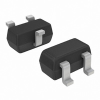
... DAP202UG SC−70 3000 / Tape & Reel (Pb−Free) DAP222T1 SC−75 3000 / Tape & Reel DAP222T1G SC−75 3000 / Tape & Reel (Pb−Free) †For information on tape and reel specifications, including part orientation and tape sizes, please refer to our Tape and Reel Packaging Specifications Brochure, BRD8011/D. ...

Page 2

ELECTRICAL CHARACTERISTICS Characteristic Symbol Reverse Voltage Leakage Current Forward Voltage Reverse Breakdown Voltage Diode Capacitance Reverse Recovery Time DAP222 DAP202U Test Circuit for DAP222 in Figure trr Test Circuit for ...

Page 3

A RECOVERY TIME EQUIVALENT TEST CIRCUIT Figure 4. Reverse Recovery Time Test Circuit for the DAP222 A RECOVERY TIME EQUIVALENT TEST CIRCUIT Figure 5. Reverse Recovery Time Test Circuit for the DAP202U DAP222, DAP202U 10% R ...

Page 4

... A1 SOLDERING FOOTPRINT* 1.803 0.071 0.508 0.020 *For additional information on our Pb−Free strategy and soldering details, please download the ON Semiconductor Soldering and Mounting Techniques Reference Manual, SOLDERRM/D. DAP222, DAP202U SC−75 (SOT−416) CASE 463−01 ISSUE F NOTES: 1. DIMENSIONING AND TOLERANCING PER ANSI Y14 ...

Page 5

... A1 *For additional information on our Pb−Free strategy and soldering details, please download the ON Semiconductor Soldering and Mounting Techniques Reference Manual, SOLDERRM/D. ON Semiconductor and are registered trademarks of Semiconductor Components Industries, LLC (SCILLC). SCILLC reserves the right to make changes without further notice to any products herein ...

Related keywords