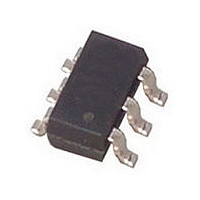
LTC4401-1ES6#TRM Linear Technology, LTC4401-1ES6#TRM Datasheet - Page 3

LTC4401-1ES6#TRM
Manufacturer Part Number
LTC4401-1ES6#TRM
Description
HF-Power Detector, ThinSOT RF Power Detector & Controller
Manufacturer
Linear Technology
Datasheet
1.LTC4401-1ES6TRM.pdf
(16 pages)
Specifications of LTC4401-1ES6#TRM
Lead Free Status / Rohs Status
Not Compliant
Available stocks
Company
Part Number
Manufacturer
Quantity
Price
PARAMETER
RF Input Frequency Range
RF Input Power Range
(LTC4401-1)
RF Input Power Range
(LTC4401-2)
RF Input Resistance
TYPICAL PERFOR A CE CHARACTERISTICS
ELECTRICAL CHARACTERISTICS
temperature range, otherwise specifications are at T
Note 1: Absolute Maximum Ratings are those values beyond which the life
of a device may be impaired.
Note 2: The LTC4401-X is guaranteed to meet performance specifications
from 0 C to 70 C. Specifications over the – 30 C to 85 C operating
temperature range are assured by design, characterization and correlation
with statistical process controls.
Note 3: Slew rate is measured open loop. The slew time at V
measured between 1V and 2V.
Note 4: Maximum DAC zero-scale offset voltage that can be applied to
PCTL.
10000
1000
100
10
1
–28
LTC4401-1 Detector Characteristics
at 900MHz
–22
75 C
25 C
–30 C
–16
RF INPUT POWER (dBm)
–10
–4
2
W
CONDITIONS
LTC4401-1 (Note 6)
LTC4401-2 (Note 6)
RF Frequency = 900MHz (Note 6)
RF Frequency = 1800MHz (Note 6)
RF Frequency = 2400MHz (Note 6)
RF Frequency = 2700MHz (Note 6)
RF Frequency = 900MHz (Note 6)
RF Frequency = 2000MHz (Note 6)
Referenced to V
8
4401 G01
U
14
CC
10000
1000
100
10
1
PCA/B
–26
A
LTC4401-1 Detector Characteristics
at 1800MHz
= 25 C. V
–20
is
The
75 C
25 C
–30 C
RF INPUT POWER (dBm)
–14
CC
denotes specifications which apply over the full operating
= 3.6V, SHDN = HI, unless otherwise noted.
–8
Note 5: This is the time from SHDN rising edge 50% switch point to
V
Note 6: Guaranteed by design. This parameter is not production tested.
Note 7: Includes maximum DAC offset voltage and maximum control
voltage.
Note 8: Bandwidth is calculated using the 10% to 90% rise time:
Note 9: Measured 12 s after SHDN = HI.
PCA
–2
BW = 0.35/rise time
= 0.25V.
4
10
4401 G02
16
LTC4401-1/LTC4401-2
10000
1000
100
10
1
–24
MIN
–28
–26
–24
–22
–28
–26
300
300
150
LTC4401-1 Detector Characteristics
at 2400MHz
–20 –16
75 C
25 C
–30 C
RF INPUT POWER (dBm)
–12 –8 –4
TYP
250
0
MAX
2700
2000
350
18
18
16
16
18
18
4
8
4401 G03
UNITS
12 16
4401fa
3
dBm
dBm
dBm
dBm
dBm
dBm
MHz
MHz


