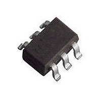
BFM505 T/R NXP Semiconductors, BFM505 T/R Datasheet

BFM505 T/R
Specifications of BFM505 T/R
Related parts for BFM505 T/R
BFM505 T/R Summary of contents
Page 1
DATA SHEET BFM505 Dual NPN wideband transistor Product specification Supersedes data of 1995 Sep 04 DISCRETE SEMICONDUCTORS 1996 Oct 08 ...
Page 2
... NXP Semiconductors Dual NPN wideband transistor FEATURES Small size Temperature and h matched FE Low noise and high gain High gain at low current and low capacitance at low voltage Gold metallization ensures excellent reliability. APPLICATIONS Oscillator and buffer amplifiers ...
Page 3
... NXP Semiconductors Dual NPN wideband transistor LIMITING VALUES In accordance with the Absolute Maximum System IEC 134. SYMBOL PARAMETER Any single transistor V collector-base voltage CBO V collector-emitter voltage CEO V emitter-base voltage EBO I DC collector current C P total power dissipation tot T storage temperature stg ...
Page 4
... NXP Semiconductors Dual NPN wideband transistor CHARACTERISTICS = 25 C unless otherwise specified SYMBOL PARAMETER DC characteristics of any single transistor V collector-base breakdown voltage (BR)CBO V collector-emitter breakdown voltage I (BR)CEO V emitter-base breakdown voltage (BR)EBO I collector-base leakage current CBO h DC current gain FE DC characteristics of the dual transistor ...
Page 5
... NXP Semiconductors Dual NPN wideband transistor 600 handbook, halfpage double loaded P tot (mW) 400 single loaded 200 100 Fig.2 Power derating as a function of soldering point temperature; typical values. 250 handbook, halfpage h FE 200 150 100 50 0 −3 −2 − Fig.4 DC current gain as a function of collector current ...
Page 6
... NXP Semiconductors Dual NPN wideband transistor 20 handbook, halfpage gain (dB MSG 900 MHz Fig.6 Gain as a function of collector current; typical values. 50 handbook, halfpage gain (dB MSG/G max mA Fig.8 Gain as a function of frequency; typical values. 1996 Oct 08 MGG199 handbook, halfpage gain (dB (mA GHz; V Fig.7 ...
Page 7
... NXP Semiconductors Dual NPN wideband transistor 5 handbook, halfpage F (dB 2000 MHz 1000 MHz 900 MHz 1 500 MHz 0 − Fig.10 Minimum noise figure as a function of collector current; typical values. 5 handbook, halfpage F (dB 1. Fig.12 Minimum noise figure as a function of frequency; typical values. 1996 Oct 08 ...
Page 8
... NXP Semiconductors Dual NPN wideband transistor APPLICATION INFORMATION SPICE parameters for any single BFM505 die SEQUENCE No. PARAMETER VALUE VAF 5 IKF 6 ISE VAR 11 IKR 12 ISC IRB 16 RBM (1) XTB 19 ( (1) 21 XTI 22 CJE 23 VJE 24 MJE XTF 27 VTF 28 ITF 29 PTF 30 CJC 31 VJC 32 MJC 33 XCJC 34 TR ...
Page 9
... NXP Semiconductors Dual NPN wideband transistor PACKAGE OUTLINE Plastic surface-mounted package; 6 leads y 6 pin 1 index DIMENSIONS (mm are the original dimensions UNIT max 1.1 0.30 0.25 mm 0.1 0.20 0.8 0.10 OUTLINE VERSION IEC SOT363 1996 Oct scale 2.2 1.35 2.2 1.3 0.65 1 ...
Page 10
... In no event shall NXP Semiconductors be liable for any indirect, incidental, punitive, special or consequential damages (including - without limitation - lost profits, lost savings, business interruption, costs related to the ...
Page 11
... NXP Semiconductors’ specifications such use shall be solely at customer’s own risk, and (c) customer fully indemnifies NXP Semiconductors for any liability, damages or failed product claims resulting from customer design and use of the product for automotive applications beyond NXP Semiconductors’ ...
Page 12
... Interface, Security and Digital Processing expertise Customer notification This data sheet was changed to reflect the new company name NXP Semiconductors, including new legal definitions and disclaimers. No changes were made to the technical content, except for package outline drawings which were updated to the latest version. ...


