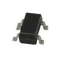
BF1109,215 NXP Semiconductors, BF1109,215 Datasheet - Page 7

BF1109,215
Manufacturer Part Number
BF1109,215
Description
RF MOSFET Small Signal Dual N-Channel 11V 30mA 200mW
Manufacturer
NXP Semiconductors
Datasheet
1.BF1109WR115.pdf
(15 pages)
Specifications of BF1109,215
Configuration
Dual
Transistor Polarity
Dual N-Channel
Drain-source Breakdown Voltage
11 V
Continuous Drain Current
30 mA
Power Dissipation
200 mW
Mounting Style
SMD/SMT
Package / Case
SOT-143B
Lead Free Status / RoHS Status
Lead free / RoHS Compliant
NXP Semiconductors
1997 Dec 08
handbook, halfpage
handbook, halfpage
N-channel dual-gate MOS-FETs
V
I
Fig.12 Input admittance as a function of frequency;
V
I
D
D
Fig.14 Forward transfer admittance and phase as
DS
DS
(mS)
(mS)
= 12 mA; T
= 12 mA; T
|y fs |
10
10
y is
10
10
= 9 V; V
= 9 V; V
10
10
−1
−2
1
1
2
2
10
10
typical values.
a function of frequency; typical values.
G2-S
G2-S
amb
amb
= 4 V.
= 4 V.
= 25 C.
= 25 C.
10
10
g is
b is
2
2
|y fs |
ϕ fs
f (MHz)
f (MHz)
MDA620
MDA622
10
10
3
3
−10
−10
−1
(deg)
ϕ fs
2
7
handbook, halfpage
handbook, halfpage
V
I
V
I
D
Fig.13 Reverse transfer admittance and phase as
D
(mS)
DS
DS
y os
|y rs |
(mS)
= 12 mA; T
= 12 mA; T
10
10
10
10
= 9 V; V
= 9 V; V
10
10
−1
−2
Fig.15 Output admittance as a function of
1
1
BF1109; BF1109R; BF1109WR
3
2
10
10
a function of frequency; typical values.
G2-S
G2-S
amb
amb
frequency; typical values.
= 4 V.
= 4 V.
= 25 C.
= 25 C.
10
10
2
2
|y rs |
b os
g os
ϕ rs
f (MHz)
f (MHz)
Product specification
MDA623
MDA621
10
10
3
−10
−10
−10
−1
3
(deg)
ϕ rs
3
2


