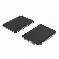
AD9860BST Analog Devices Inc, AD9860BST Datasheet - Page 4

AD9860BST
Manufacturer Part Number
AD9860BST
Description
IC FRONT-END MIXED-SGNL 128-LQFP
Manufacturer
Analog Devices Inc
Datasheet
1.AD9860BST.pdf
(32 pages)
Specifications of AD9860BST
Rohs Status
RoHS non-compliant
Rf Type
LMDS, MMDS
Features
10-bit ADCs, 12-bit DACs
Package / Case
128-LQFP
Operating Supply Voltage (max)
3.9V
Operating Temp Range
-40C to 70C
Operating Temperature Classification
Commercial
Package Type
LQFP
Mounting
Surface Mount
Pin Count
128
Lead Free Status / RoHS Status
Not Compliant
Available stocks
Company
Part Number
Manufacturer
Quantity
Price
Company:
Part Number:
AD9860BSTZ
Manufacturer:
ADI
Quantity:
285
AD9860/AD9862
TIMING CHARACTERISTICS
(20 pF Load)
Minimum Reset Pulsewidth Low (t
Digital Output Rise/Fall Time
DLL Output Clock
DLL Output Duty Cycle
AUXILARY ADC
AUXILARY DAC
ADC TIMING
DAC Timing
Specifications subject to change without notice.
PARAMETERS (continued)
POWER SUPPLY (continued)
NOTES
1
2
Specifications subject to change without notice.
% f
Interpolation filter stop band is defined by image suppression of 50 dB or greater.
Tx–/Rx–Interface (See Figures 11 and 12)
Serial Control Bus (See Figures 1 and 2)
Conversion Rate
Input Range
Resolution
Settling Time
Output Range
Resolution
Latency (All Digital Processing Blocks Disabled)
Latency (All Digital Processing Blocks Disabled)
Latency (2
Latency (4
Additional Latency (Hilbert Filter Enabled)
Additional Latency (Coarse Modulation Enabled)
Additional Latency (Fine Modulation Enabled)
Output Settling Time (TST) (to 0.1%)
Rx Path (f
DATA
TxSYNC/TxIQ Setup Time (t
TxSYNC/TxIQ Hold Time (t
RxSYNC/RxIQ/IF to Valid Time(t
RxSYNC/RxIQ/IF Hold Time (t
Maximum SCLK Frequency (f
Minimum Clock Pulsewidth High (t
Minimum Clock Pulsewidth Low (t
Maximum Clock Rise/Fall Time
Minimum Data/SEN Setup Time (t
Minimum SEN/Data Hold Time (t
Minimum Data/SCLK Setup Time (t
Minimum Data Hold Time (t
Output Data Valid/SCLK Time (t
Processing Blocks Disabled
Decimation Filter Enabled
Hilbert Filter Enabled
Hilbert and Decimation Filter Enabled
refers to the input data rate of the digital block.
ADC
Interpolation Enabled)
Interpolation Enabled)
= 64 MSPS)
DH
Tx2
RL
Tx1
SCLK
)
)
, t
Rx2
, t
DV
Tx4
Rx1
H
)
Tx3
, t
LOW
S
HI
)
)
)
)
, t
Rx4
DS
)
)
)
Rx3
)
)
)
Temp
NA
25ºC
25ºC
25ºC
25ºC
25ºC
25ºC
25ºC
Full
Full
Full
Full
Full
Full
Full
Full
Full
25ºC
25ºC
25ºC
25ºC
25ºC
25ºC
25ºC
25ºC
25ºC
25ºC
25ºC
25ºC
25ºC
25ºC
Temp
25ºC
25ºC
25ºC
25ºC
–4–
Test
Level
NA
III
III
III
III
III
III
III
III
III
III
III
III
III
III
III
III
III
III
III
III
III
III
III
III
III
III
III
III
III
III
Test
Level
III
III
III
III
Min
5
2.8
32
3
3
0.2
30
30
25
0
25
0
Min
AD9860/AD9862
Typ
50
3
10
8
3
8
7
3
30
72
36
5
8
35
1.25
AD9860/AD9862
Typ
9
15
16
18.5
Max
4
128
5.2
16
1
30
Max
Unit
Clock Cycles
ns
MHz
%
ns
ns
ns
ns
MHz
ns
ns
ms
ns
ns
ns
ns
ns
MHz
V
Bits
ms
V
Bits
Cycles
Cycles
Cycles
Cycles
Cycles
Cycles
Cycles
ns
Unit
mA
mA
mA
mA
REV. 0


