AD9860BST Analog Devices Inc, AD9860BST Datasheet - Page 2
AD9860BST
Manufacturer Part Number
AD9860BST
Description
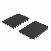
IC FRONT-END MIXED-SGNL 128-LQFP
Manufacturer
Analog Devices Inc
Datasheet
1.AD9860BST.pdf
(32 pages)
Specifications of AD9860BST
Rohs Status
RoHS non-compliant
Rf Type
LMDS, MMDS
Features
10-bit ADCs, 12-bit DACs
Package / Case
128-LQFP
Operating Supply Voltage (max)
3.9V
Operating Temp Range
-40C to 70C
Operating Temperature Classification
Commercial
Package Type
LQFP
Mounting
Surface Mount
Pin Count
128
Lead Free Status / RoHS Status
Not Compliant
Available stocks
Company
Part Number
Manufacturer
Quantity
Price

Company:
Part Number:
AD9860BSTZ
Manufacturer:
ADI
Quantity:
285


AD9860/AD9862–SPECIFICATIONS
Tx PARAMETERS
12-/14-BIT DAC CHARACTERISTICS
TRANSMIT TxPGA CHARACTERISTICS
Tx DIGITAL FILTER CHARACTERISTICS
DYNAMIC PERFORMANCE (A
Rx PARAMETERS
RECEIVE BUFFER
RECEIVE PGA CHARACTERISTICS
10-/12-BIT ADC CHARACTERISTICS
Resolution
Maximum Update Rate
Full-Scale Output Current
Gain Error (Using Internal Reference)
Offset Error
Reference Voltage (REFIO Level)
Negative Differential Nonlinearity (–DNL)
Positive Differential Nonlinearity (+DNL)
Integral Nonlinearity (INL)
Output Capacitance
Phase Noise @ 1 kHz Offset, 6 MHz Tone
Output Voltage Compliance Range
Gain Range
Step Size Accuracy
Step Size
Hilbert Filter Pass Band (<0.1 dB Ripple)
2 /4
Differential Phase
Differential Gain
AD9860 Signal-to-Noise Ratio (SNR)
AD9860 Signal-to-Noise and Distortion Ratio
AD9860 Total Harmonic Distortion (THD)
AD9860 Wideband SFDR (to Nyquist)
AD9860 Narrowband SFDR (1 MHz Window)
AD9862 Signal-to-Noise Ratio (SNR)
AD9862 Signal-to-Noise and Distortion Ratio
AD9862 Total Harmonic Distortion (THD)
AD9862 Wideband SFDR (to Nyquist)
AD9862 Narrowband SFDR (1 MHz Window)
Input Resistance (Differential)
Input Capacitance (Each Input)
Maximum Input Bandwidth (–3 dB)
Analog Input Range (Best Noise Performance)
Analog Input Range (Best THD Performance)
Gain Error
Gain Range
Step Size Accuracy
Step Size
Input Bandwidth (–3 dB, Rx Buffer Bypassed)
Resolution
Maximum Conversion Rate
Crystal and OSC IN Multiplier Enabled at 4
1 MHz Analog Out, I
1 MHz Analog Out, I
6 MHz Analog Out, I
1 MHz Analog Out, I
1 MHz Analog Out, I
1 MHz Analog Out, I
1 MHz Analog Out, I
6 MHz Analog Out, I
1 MHz Analog Out, I
1 MHz Analog Out, I
Interpolator Stop Band
OUT
OUT
OUT
OUT
OUT
OUT
OUT
OUT
OUT
OUT
= 2 mA
= 20 mA
= 20 mA
= 2 mA
= 20 mA
= 2 mA
= 20 mA
= 20 mA
= 2 mA
= 20 mA
2
OUT
= 20 mA FS, f = 1 MHz)
Temp
NA
25ºC
25ºC
25ºC
25ºC
25ºC
25ºC
25ºC
25ºC
Full
25ºC
25ºC
25ºC
Full
Full
25ºC
25ºC
Full
25ºC
25ºC
25ºC
25ºC
25ºC
25ºC
25ºC
25ºC
25ºC
25ºC
Full
Full
Full
Full
25ºC
25ºC
25ºC
25ºC
25ºC
NA
Full
Full
Full
Full
Full
Full
Full
Full
–2–
(V
Normal Timing Mode, 2
RxPGA = +6 dB Gain, TxPGA = +20 dB Gain.)
A
Test
Level
NA
I
I
I
I
III
III
III
III
III
II
III
III
III
II
II
III
III
I
I
I
III
I
III
III
I
I
I
I
III
I
III
III
I
III
III
III
II
II
I
I
I
I
III
NA
I
= 3.3 V
5%, V
Min
128
2
–5.5
–1
1.15
–0.5
12.5
68.2
62.5
64.4
83
68.9
64.75
64.9
83
19
64
D
= 3.3 V
AD9860/AD9862
DLL Setting, R
Typ
12/14
+0.5
0.0
1.22
–0.5/–0.5
1/2
± 1/± 3
5
–115
20
± 0.1
0.08
<0.1
<1
70.7
66.1
–74.5
70.6
75
75
70.2
90
72.0
69.8
–75.5
70.6
76.0
76.0
70.2
90
200
5
140
2
1
± 0.3
20
± 0.2
1
250
10/12
10%, f
DAC
SET
= 128 MHz, f
= 4 k , 50
Max
20
+5.5
+1
1.28
+1.5
38
± 38
–64.0
–65.0
21
ADC
DAC Load,
= 64 MHz
Unit
Bits
MSPS
mA
%FS
%FS
V
LSB
LSB
LSB
pF
dBc/Hz
V
dB
dB
dB
% f
% f
Degree
LSB
dB
dB
dB
dBc
dBc
dBc
dBc
dBc
dB
dB
dB
dBc
dBc
dBc
dBc
dBc
W
pF
MHz
V p-p Diff
V p-p Diff
dB
dB
dB
dB
MHz
Bits
MHz
REV. 0
DATA
DATA
1
Related parts for AD9860BST
Image
Part Number
Description
Manufacturer
Datasheet
Request
R

Part Number:
Description:
BOARD EVALUATION FOR AD9860
Manufacturer:
Analog Devices Inc
Datasheet:

Part Number:
Description:
±1.7g Dual-Axis IMEMS Accelerometer Evaluation Board
Manufacturer:
Analog Devices Inc
Datasheet:
Part Number:
Description:
Inertial Sensor Evaluation System
Manufacturer:
Analog Devices Inc
Datasheet:
Part Number:
Description:
Manufacturer:
Analog Devices Inc
Datasheet:
Part Number:
Description:
Manufacturer:
Analog Devices Inc
Datasheet:
Part Number:
Description:
Manufacturer:
Analog Devices Inc
Datasheet:
Part Number:
Description:
Manufacturer:
Analog Devices Inc
Datasheet:
Part Number:
Description:
Manufacturer:
Analog Devices Inc
Datasheet:
Part Number:
Description:
Manufacturer:
Analog Devices Inc
Datasheet:
Part Number:
Description:
Manufacturer:
Analog Devices Inc
Datasheet:
Part Number:
Description:
Manufacturer:
Analog Devices Inc
Datasheet:
Part Number:
Description:
Manufacturer:
Analog Devices Inc
Datasheet:
Part Number:
Description:
Manufacturer:
Analog Devices Inc
Datasheet: