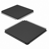
CY7C056V-15AXC Cypress Semiconductor Corp, CY7C056V-15AXC Datasheet - Page 21

CY7C056V-15AXC
Manufacturer Part Number
CY7C056V-15AXC
Description
CY7C056V-15AXC
Manufacturer
Cypress Semiconductor Corp
Datasheet
1.CY7C057V-15BBC.pdf
(26 pages)
Specifications of CY7C056V-15AXC
Format - Memory
RAM
Memory Type
SRAM - Dual Port, Asynchronous
Memory Size
576K (16K x 36)
Speed
15ns
Interface
Parallel
Voltage - Supply
3 V ~ 3.6 V
Operating Temperature
0°C ~ 70°C
Package / Case
144-LQFP
Lead Free Status / RoHS Status
Lead free / RoHS Compliant
Available stocks
Company
Part Number
Manufacturer
Quantity
Price
Company:
Part Number:
CY7C056V-15AXC
Manufacturer:
Cypress Semiconductor Corp
Quantity:
10 000
pin and to the bus size select (SIZE) pin will select long-word
(36-bit) operation. A logic “1” level applied to the bus match
select (BM) pin will enable either byte or word bus width
operation on the right port I/Os depending on the logic level
applied to the SIZE pin. The level of bus match select (BM) must
be static throughout device operation.
Normally, the bus size select (SIZE) pin would have no
standard-cycle application when BM = LOW and the device is in
long-word (36-bit) operation. A “special” mode has been added
however to disable ALL right port I/Os while the chip is active.
This I/O disable mode is implemented when SIZE is forced to a
logic “1” while BM is at a logic “0”. It allows the bus-matched port
to support a chip enable “Don’t care” semaphore read/write
access similar to that provided on the left port of the device when
all Byte Select (B
The bus size select (SIZE) pin selects either a byte or word data
arrangement on the right port when the bus match select (BM)
pin is HIGH. A logic “1” on the SIZE pin when the BM pin is HIGH
selects a byte bus (9-bit) data arrangement). A logic “0” on the
SIZE pin when the BM pin is HIGH selects a word bus (18-bit)
data arrangement. The level of the bus size select (SIZE) must
also be static throughout normal device operation.
Long-Word (36-bit) Operation
Bus match select (BM) and bus size select (SIZE) set to a logic
“0” will enable standard cycle long-word (36-bit) operation. In this
mode, the right port’s I/O operates essentially in an identical
fashion as does the left port of the dual-port SRAM. However no
byte select control is available. All 36 bits of the long-word are
shifted into and out of the right port’s I/O buffer stages. All read
and write timing parameters may be identical with respect to the
two data ports. When the right port is configured for a long-word
size, word address (WA), and byte Address (BA) pins have no
application and their inputs are “Don’t Care”
user.
Note
Document #: 38-06055 Rev. *E
55. Even though a logic level applied to a “Don’t Care” input will not change the logical operation of the dual-port, inputs that are temporarily a “Don’t Care” (along with
unused inputs) must not be allowed to float. They must be forced either HIGH or LOW.
0–3
) control inputs are deselected.
[55]
for the external
Word (18-bit) Operation
Word (18-bit) bus sizing operation is enabled when bus match
select (BM) is set to a logic “1” and the bus sze select (SIZE) pin
is set to a logic “0.” In this mode, 18 bits of data are ported
through I/O
pin during word bus size operation determines whether the
most-significant or least-significant data bits are ported through
the I/O
(note that when the right port is configured for word size
operation, the Byte Address pin has no application and its input
is “Don’t care”
Device operation is accomplished by treating the WA pin as an
additional address input and using standard cycle address and
data setup/hold times. When transferring data in word (18-bit)
bus match format, the unused I/O
Byte (9-bit) Operation
Byte (9-bit) bus sizing operation is enabled when bus match
select (BM) is set to a logic “1” and the bus size select (SIZE) pin
is set to a logic “1.” In this mode, data is ported through I/O
in four groups of 9-bit bytes. A particular 9-bit byte group is
selected according to the levels applied to the word address
(WA) and byte address (BA) input pins.
Device operation is accomplished by treating the word address
(WA) pin and the byte address (BA) pins as additional address
inputs having standard cycle address and data set-up/hold
times. When transferring data in byte (9-bit) bus match format,
the unused I/O
I/O
I/O
I/O
I/O
27R–35R
18R–26R
I/Os
0R–17R
9R–17R
0R–8R
0R–17R
[55]
pins in an Upper word/Lower word select fashion
9R–35R
).
. The level applied to the word address (WA)
Upper-MSB
Lower-MSB
Upper-MSB
Lower-MSB
pins are three-stated.
Rank
18R–35R
WA
pins are three-stated.
1
1
0
0
CY7C056V
CY7C057V
Page 21 of 26
BA
1
0
1
0
0R–8R
[+] Feedback


