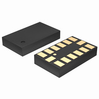
ADXL345BCCZ-RL Analog Devices Inc, ADXL345BCCZ-RL Datasheet - Page 14
ADXL345BCCZ-RL
Manufacturer Part Number
ADXL345BCCZ-RL
Description
Digital Output Three-Axis Accel 4K RL
Manufacturer
Analog Devices Inc
Series
iMEMS®r
Datasheet
1.EVAL-ADXL345Z.pdf
(40 pages)
Specifications of ADXL345BCCZ-RL
Design Resources
Sensing Low-g Acceleration Using ADXL345 Digital Accelerometer Connected to ADuC7024 (CN0133)
Axis
X, Y, Z
Acceleration Range
±2g, 4g, 8g, 16g
Sensitivity
256LSB/g, 128LSB/g, 64LSB/g, 32LSB/g
Voltage - Supply
2 V ~ 3.6 V
Output Type
Digital
Bandwidth
6.25Hz ~ 3.2kHz Selectable
Interface
I²C, SPI
Mounting Type
Surface Mount
Package / Case
14-LGA
Package Type
LGA
Operating Supply Voltage (typ)
2.5V
Operating Supply Voltage (max)
3.6V
Operating Temperature (min)
-40C
Operating Temperature (max)
85C
Operating Temperature Classification
Industrial
Product Depth (mm)
3mm
Product Length (mm)
5mm
Mounting
Surface Mount
Pin Count
14
Lead Free Status / RoHS Status
Lead free / RoHS Compliant
Lead Free Status / RoHS Status
Lead free / RoHS Compliant
Other names
ADXL345BCCZ-RLTR
Available stocks
Company
Part Number
Manufacturer
Quantity
Price
Company:

Part Number:
ADXL345BCCZ-RL7
Manufacturer:
POWER
Quantity:
14 300


ADXL345
POWER SAVINGS
Power Modes
The ADXL345 automatically modulates its power consumption
in proportion to its output data rate, as outlined in Table 7. If
additional power savings is desired, a lower power mode is
available. In this mode, the internal sampling rate is reduced,
allowing for power savings in the 12.5 Hz to 400 Hz data rate
range at the expense of slightly greater noise. To enter low power
mode, set the LOW_POWER bit (Bit 4) in the BW_RATE register
(Address 0x2C). The current consumption in low power mode
is shown in Table 8 for cases where there is an advantage to
using low power mode. Use of low power mode for a data rate
not shown in Table 8 does not provide any advantage over the same
data rate in normal power mode. Therefore, it is recommended
that only data rates shown in Table 8 are used in low power mode.
The current consumption values shown in Table 7 and Table 8
are for a V
Table 7. Typical Current Consumption vs. Data Rate
(T
Output Data
Rate (Hz)
3200
1600
800
400
200
100
50
25
12.5
6.25
3.13
1.56
0.78
0.39
0.20
0.10
A
= 25°C, V
S
of 2.5 V.
S
= 2.5 V, V
Bandwidth (Hz)
1600
800
400
200
100
50
25
12.5
6.25
3.13
1.56
0.78
0.39
0.20
0.10
0.05
DD I/O
= 1.8 V)
Rate Code
1111
1110
1101
1100
1011
1010
1001
1000
0111
0110
0101
0100
0011
0010
0001
0000
I
140
90
140
140
140
140
90
60
50
45
40
34
23
23
23
23
DD
(μA)
Rev. B | Page 14 of 40
Table 8. Typical Current Consumption vs. Data Rate,
Low Power Mode (T
Output Data
Rate (Hz)
400
200
100
50
25
12.5
Auto Sleep Mode
Additional power can be saved if the ADXL345 automatically
switches to sleep mode during periods of inactivity. To enable
this feature, set the THRESH_INACT register (Address 0x25)
and the TIME_INACT register (Address 0x26) each to a value
that signifies inactivity (the appropriate value depends on the
application), and then set the AUTO_SLEEP bit (Bit D4) and the
link bit (Bit D5) in the POWER_CTL register (Address 0x2D).
Current consumption at the sub-12.5 Hz data rates that are
used in this mode is typically 23 μA for a V
Standby Mode
For even lower power operation, standby mode can be used. In
standby mode, current consumption is reduced to 0.1 μA (typical).
In this mode, no measurements are made. Standby mode is
entered by clearing the measure bit (Bit D3) in the POWER_CTL
register (Address 0x2D). Placing the device into standby mode
preserves the contents of FIFO.
Bandwidth (Hz)
200
100
50
25
12.5
6.25
A
= 25°C, V
S
= 2.5 V, V
Rate Code
1100
1011
1010
1001
1000
0111
S
DD I/O
of 2.5 V.
= 1.8 V)
I
90
60
50
45
40
34
DD
(μA)
Related parts for ADXL345BCCZ-RL
Image
Part Number
Description
Manufacturer
Datasheet
Request
R

Part Number:
Description:
±1.7g Dual-Axis IMEMS Accelerometer Evaluation Board
Manufacturer:
Analog Devices Inc
Datasheet:

Part Number:
Description:
Inertial Sensor Evaluation System
Manufacturer:
Analog Devices Inc
Datasheet:
Part Number:
Description:
Manufacturer:
Analog Devices Inc
Datasheet:
Part Number:
Description:
Manufacturer:
Analog Devices Inc
Datasheet:
Part Number:
Description:
Manufacturer:
Analog Devices Inc
Datasheet:
Part Number:
Description:
Manufacturer:
Analog Devices Inc
Datasheet:
Part Number:
Description:
Manufacturer:
Analog Devices Inc
Datasheet:
Part Number:
Description:
Manufacturer:
Analog Devices Inc
Datasheet:
Part Number:
Description:
Manufacturer:
Analog Devices Inc
Datasheet:
Part Number:
Description:
Manufacturer:
Analog Devices Inc
Datasheet:
Part Number:
Description:
Manufacturer:
Analog Devices Inc
Datasheet:
Part Number:
Description:
Manufacturer:
Analog Devices Inc
Datasheet:
Part Number:
Description:
Manufacturer:
Analog Devices Inc
Datasheet: