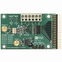
AD9236BCP-80EB Analog Devices Inc, AD9236BCP-80EB Datasheet - Page 17

AD9236BCP-80EB
Manufacturer Part Number
AD9236BCP-80EB
Description
12-BIT 3V 80 MSPS A-D CONVERTER
Manufacturer
Analog Devices Inc
Datasheet
1.AD9236BCPZRL7-80.pdf
(36 pages)
Specifications of AD9236BCP-80EB
Number Of Adc's
1
Number Of Bits
12
Sampling Rate (per Second)
80M
Data Interface
Parallel
Inputs Per Adc
1 Differential
Input Range
2 Vpp
Power (typ) @ Conditions
366mW @ 80MSPS
Voltage Supply Source
Single Supply
Operating Temperature
-40°C ~ 85°C
Utilized Ic / Part
AD9236-80
Lead Free Status / RoHS Status
Contains lead / RoHS non-compliant
TIMING
The AD9236 provides latched data outputs with a pipeline delay
of seven clock cycles. Data outputs are available one propagation
delay (t
Figure 2 for a detailed timing diagram.
The length of the output data lines and the loads placed on
them should be minimized to reduce transients within the
AD9236. These transients can degrade the converter’s dynamic
performance.
The lowest typical conversion rate of the AD9236 is 1 MSPS. At
clock rates below 1 MSPS, dynamic performance can degrade.
VOLTAGE REFERENCE
A stable and accurate 0.5 V voltage reference is built into the
AD9236. The input range can be adjusted by varying the
reference voltage applied to the AD9236 using either the
internal reference or an externally applied reference voltage.
The input span of the ADC tracks reference voltage changes
linearly. The various reference modes are summarized in Table 10
and described in the following sections.
If the ADC is being driven differentially through a transformer,
the reference voltage can be used to bias the center tap
(common-mode voltage).
Internal Reference Connection
A comparator within the AD9236 detects the potential at the
SENSE pin and configures the reference into four possible
states, which are summarized in Table 10. If SENSE is
grounded, the reference amplifier switch is connected to the
internal resistor divider (see Figure 33), setting VREF to 1 V.
Connecting the SENSE pin to VREF switches the reference
amplifier output to the SENSE pin, completing the loop and
providing a 0.5 V reference output. If a resistor divider is
connected as shown in Figure 34, the switch is again set to the
SENSE pin. This puts the reference amplifier in a noninverting
mode with the VREF output defined as follows:
Table 10. Reference Configuration Summary
Selected Mode
External Reference
Internal Fixed Reference
Programmable Reference
Internal Fixed Reference
VREF
PD
) after the rising edge of the clock signal. Refer to
=
0
5 .
×
⎛ +
⎜
⎝
1
R2
R1
⎞
⎟
⎠
SENSE Voltage
AVDD
VREF
0.2 V to VREF
AGND to 0.2 V
Resulting VREF (V)
N/A
0.5
1.0
0
5 .
×
Rev. B | Page 17 of 36
⎛ +
⎜
⎝
1
R2
R1
⎞
⎟
⎠
(See Figure 34)
In all reference configurations, REFT and REFB drive the A/D
conversion core and establish its input span. The input range of
the ADC always equals twice the voltage at the reference pin for
either an internal or an external reference.
10μF
10μF
+
+
0.1μF
0.1μF
SENSE
Figure 34. Programmable Reference Configuration
VREF
VIN+
VIN–
Figure 33. Internal Reference Configuration
R2
SENSE
R1
VREF
VIN+
VIN–
Resulting Differential Span (V p-p)
2 × External Reference
1.0
2 × VREF
2.0
SELECT
LOGIC
AD9236
SELECT
LOGIC
AD9236
0.5V
CORE
ADC
03066-A-017
0.5V
CORE
ADC
03066-0-018
REFT
REFB
0.1μF
0.1μF
0.1μF
REFT
REFB
AD9236
0.1μF
0.1μF
0.1μF
+
10μF
+
10μF


