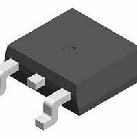
STGD7NB60S STMicroelectronics, STGD7NB60S Datasheet

STGD7NB60S
Specifications of STGD7NB60S
Available stocks
Related parts for STGD7NB60S
STGD7NB60S Summary of contents
Page 1
... Max. Operating Junction Temperature Pulse width limited by safe operating area November 1999 N-CHANNEL 7A - 600V DPAK V I CE(sat) C < 1 cesat with outstanding = 100 STGD7NB60S Power MESH 3 1 DPAK TO-252 (Suffix "T4") INTERNAL SCHEMATIC DIAGRAM Value 600 0.44 -65 to 150 150 IGBT Unit ...
Page 2
... STGD7NB60S THERMAL DATA R Thermal Resistance Junction-case thj-case R Thermal Resistance Junction-ambient thj-amb R Thermal Resistance Case-sink thc-sink ELECTRICAL CHARACTERISTICS (T OFF Symbol Parameter V Collector-Emitter BR(CES) Breakdown Voltage V Emitter-Collector BR(ECR) Breakdown Voltage I Collector cut-off CES ( Gate-Emitter Leakage GES Current ( Symbol Parameter V Gate Threshold GE(th) Voltage ...
Page 3
... Pulse width limited by safe operating area ( ) Pulsed: Pulse duration = 300 s, duty cycle 1.5 % (**)Losses Include Also The Tail (Jedec Standardization) Thermal Impedance Test Conditions V = 480 100 480 100 125 C j STGD7NB60S Min. Typ. Max. Unit 2.2 s 1.2 s 1.2 s 3.5 mJ 3.8 s 1.2 s 1.9 s 5.3 mJ 3/8 ...
Page 4
... STGD7NB60S Output Characteristics Transconductance Collector-Emitter On Voltage vs Collector Current 4/8 Transfer Characteristics Collector-Emitter On Voltage vs Temperature Gate Threshold vs Temperature ...
Page 5
... Normalized Breakdown Voltage vs Temperature Gate Charge vs Gate-Emitter Voltage Off Losses vs Temperature Capacitance Variations Off Losses vs Gate Resistance Off Losses vs Collector Current STGD7NB60S 5/8 ...
Page 6
... STGD7NB60S Switching Off Safe Operatin Area Fig. 1: Gate Charge test Circuit Fig. 3: Switching Waveforms 6/8 Fig. 2: Test Circuit For Inductive Load Switching ...
Page 7
... STGD7NB60S inch TYP. MAX. 0.094 0.043 0.009 0.035 0.212 0.023 0.023 0.244 0.260 0.181 0.397 0.031 0.039 DETAIL "A" 0068772-B 7/8 ...
Page 8
... STGD7NB60S Information furnished is believed to be accurate and reliable. However, STMicroelectronics assumes no responsibility for the consequences of use of such information nor for any infringement of patents or other rights of third parties which may result from its use. No license is granted by implication or otherwise under any patent or patent rights of STMicroelectronics. Specification mentioned in this publication are subject to change without notice ...


