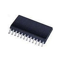
PCA9552D NXP Semiconductors, PCA9552D Datasheet - Page 24

PCA9552D
Manufacturer Part Number
PCA9552D
Description
LED Drivers I2C LED BLINKR 16BIT
Manufacturer
NXP Semiconductors
Datasheet
1.PCA9552BS118.pdf
(28 pages)
Specifications of PCA9552D
Number Of Segments
16
Low Level Output Current
25000 uA (Min)
Operating Supply Voltage
2.3 V to 5.5 V
Maximum Supply Current
550 uA
Maximum Power Dissipation
400 mW
Maximum Operating Temperature
+ 85 C
Mounting Style
SMD/SMT
Package / Case
SOT-137
Minimum Operating Temperature
- 40 C
Lead Free Status / RoHS Status
Lead free / RoHS Compliant
Other names
PCA9552D,112
Available stocks
Company
Part Number
Manufacturer
Quantity
Price
Part Number:
PCA9552D
Manufacturer:
PHILIPS/飞利浦
Quantity:
20 000
Part Number:
PCA9552D,118
Manufacturer:
NXP/恩智浦
Quantity:
20 000
Company:
Part Number:
PCA9552D118
Manufacturer:
NXP Semiconductors
Quantity:
1 990
Company:
Part Number:
PCA9552DЈ¬112
Manufacturer:
NXP
Quantity:
1 570
Philips Semiconductors
PCA9552_5
Product data sheet
15.4 Manual soldering
15.5 Package related soldering information
During placement and before soldering, the package must be fixed with a droplet of
adhesive. The adhesive can be applied by screen printing, pin transfer or syringe
dispensing. The package can be soldered after the adhesive is cured.
Typical dwell time of the leads in the wave ranges from 3 seconds to 4 seconds at 250 C
or 265 C, depending on solder material applied, SnPb or Pb-free respectively.
A mildly-activated flux will eliminate the need for removal of corrosive residues in most
applications.
Fix the component by first soldering two diagonally-opposite end leads. Use a low voltage
(24 V or less) soldering iron applied to the flat part of the lead. Contact time must be
limited to 10 seconds at up to 300 C.
When using a dedicated tool, all other leads can be soldered in one operation within
2 seconds to 5 seconds between 270 C and 320 C.
Table 15:
[1]
Package
BGA, HTSSON..T
SSOP..T
DHVQFN, HBCC, HBGA, HLQFP, HSO, HSOP,
HSQFP, HSSON, HTQFP, HTSSOP, HVQFN,
HVSON, SMS
PLCC
LQFP, QFP, TQFP
SSOP, TSSOP, VSO, VSSOP
CWQCCN..L
•
•
•
Use a double-wave soldering method comprising a turbulent wave with high upward
pressure followed by a smooth laminar wave.
For packages with leads on two sides and a pitch (e):
– larger than or equal to 1.27 mm, the footprint longitudinal axis is preferred to be
– smaller than 1.27 mm, the footprint longitudinal axis must be parallel to the
The footprint must incorporate solder thieves at the downstream end.
For packages with leads on four sides, the footprint must be placed at a 45 angle to
the transport direction of the printed-circuit board. The footprint must incorporate
solder thieves downstream and at the side corners.
For more detailed information on the BGA packages refer to the (LF)BGA Application Note (AN01026);
order a copy from your Philips Semiconductors sales office.
[5]
parallel to the transport direction of the printed-circuit board;
transport direction of the printed-circuit board.
, SO, SOJ
[3]
[1]
, TFBGA, VFBGA, XSON
Suitability of surface mount IC packages for wave and reflow soldering methods
[8]
, PMFP
[3]
, LBGA, LFBGA, SQFP,
[9]
, WQCCN..L
Rev. 05 — 9 March 2006
16-bit I
[8]
2
C-bus LED driver with programmable blink rates
Soldering method
Wave
not suitable
not suitable
suitable
not recommended
not recommended
not suitable
[4]
© Koninklijke Philips Electronics N.V. 2006. All rights reserved.
[5] [6]
[7]
PCA9552
Reflow
suitable
suitable
suitable
suitable
suitable
not suitable
[2]
24 of 28


