PCA9552D NXP Semiconductors, PCA9552D Datasheet
PCA9552D
Specifications of PCA9552D
Available stocks


Related parts for PCA9552D


PCA9552D Summary of contents
Page 1
PCA9552 16-bit I Rev. 05 — 9 March 2006 1. General description The PCA9552 LED blinker blinks LEDs in I necessary to limit bus traffic or free up the I etc.) timer. The uniqueness of this device is the internal ...
Page 2
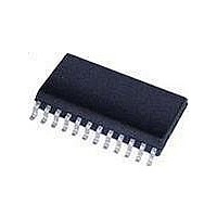
... JESD22-A115 and 1000 V CDM per JESD22-C101 Latch-up testing is done to JEDEC Standard JESD78 which exceeds 100 mA Packages offered: SO24, TSSOP24, HVQFN24 3. Ordering information Table 1: Ordering information +85 C amb Type number Topside mark Package PCA9552D PCA9552D PCA9552PW PCA9552 PCA9552BS 9552 4. Block diagram PCA9552 SCL INPUT FILTERS SDA V ...
Page 3
... Fig 4. Pin configuration for HVQFN24 PCA9552_5 Product data sheet 2 16-bit I C-bus LED driver with programmable blink rates SDA 3 22 SCL 4 21 RESET 5 20 LED15 6 19 LED14 PCA9552D 7 18 LED13 8 17 LED12 9 16 LED11 10 15 LED10 11 14 LED9 12 13 LED8 SS 002aac165 terminal 1 index area 1 LED0 ...
Page 4
Philips Semiconductors 5.2 Pin description Table 2: Symbol LED0 LED1 LED2 LED3 LED4 LED5 LED6 LED7 V SS LED8 LED9 LED10 LED11 LED12 LED13 LED14 LED15 RESET SCL SDA V DD [1] HVQFN package die supply ground ...
Page 5
Philips Semiconductors 6. Functional description Refer to 6.1 Device address Following a START condition, the bus master must output the address of the slave it is accessing. The address of the PCA9552 is shown in internal pull-up resistors are incorporated ...
Page 6
Philips Semiconductors 6.2.1 Control Register definition Table 6.3 Register descriptions 6.3.1 INPUT0 - Input register 0 The ...
Page 7
Philips Semiconductors 6.3.3 PCS0 - Frequency Prescaler 0 PSC0 is used to program the period of the PWM output. The period of BLINK0 = (PSC0 + 1) / 44. Table 6: Bit Symbol Default 6.3.4 PWM0 - Pulse Width Modulation ...
Page 8
Philips Semiconductors 6.3.7 LS0 to LS3 - LED selector registers The LSn LED select registers determine the source of the LED data output is set LOW (LED on output is set high-impedance (LED off; default) 10 ...
Page 9
Philips Semiconductors 6.4 Pins used as GPIOs LED pins not used to control LEDs can be used as general purpose I/Os (GPIOs). For use as input, set LEDn to high-impedance (01) and then read the pin state via the input ...
Page 10
Philips Semiconductors 7. Characteristics of the I 2 The I C-bus is for 2-way, 2-line communication between different ICs or modules. The two lines are a serial data line (SDA) and a serial clock line (SCL). Both lines must be ...
Page 11
Philips Semiconductors SDA SCL MASTER TRANSMITTER/ RECEIVER Fig 9. System configuration 7.3 Acknowledge The number of data bytes transferred between the START and the STOP conditions from transmitter to receiver is not limited. Each byte of eight bits is followed ...
Page 12
Philips Semiconductors 7.4 Bus transactions SCL slave address SDA START condition write to register data out from port Fig 11. Write to register slave address SDA ...
Page 13
Philips Semiconductors 8. Application design-in information C-BUS/SMBus (3 ) MASTER SDA SCL LED0 to LED12 are used as LED drivers. LED13 to LED15 are used as regular GPIOs. Fig 14. Typical application 8.1 Minimizing ...
Page 14
Philips Semiconductors Fig 15. High value resistor in parallel with 8.2 Programming example The following example will show how to set LED0 to LED3 on. It will then set LED4 and LED5 to blink ...
Page 15
Philips Semiconductors 9. Limiting values Table 12: Limiting values In accordance with the Absolute Maximum Rating System (IEC 60134). Symbol Parameter V supply voltage DD V voltage on an input/output pin I/O I output current on pin LEDn O(LEDn) I ...
Page 16
Philips Semiconductors Table 13: Static characteristics amb Symbol Parameter Select inputs A0, A1, A2; RESET V LOW-level input voltage IL V HIGH-level input voltage IH I ...
Page 17
Philips Semiconductors 11. Dynamic characteristics Table 14: Dynamic characteristics Symbol Parameter f SCL clock frequency SCL t bus free time between a STOP and BUF START condition t hold time (repeated) START condition HD;STA t set-up time for a repeated ...
Page 18
Philips Semiconductors SDA t BUF t LOW SCL t HD;STA P S Fig 19. Definition of timing on the I START protocol condition (S) t SU;STA SCL t BUF SDA t HD;STA Rise and fall times refer ...
Page 19
Philips Semiconductors 12. Test information Fig 22. Test circuitry for switching times PCA9552_5 Product data sheet 2 16-bit I C-bus LED driver with programmable blink rates V I PULSE GENERATOR R = load resistor for LEDn. R for SDA and ...
Page 20
Philips Semiconductors 13. Package outline SO24: plastic small outline package; 24 leads; body width 7 pin 1 index 1 e DIMENSIONS (inch dimensions are derived from the original mm dimensions) A UNIT ...
Page 21
Philips Semiconductors TSSOP24: plastic thin shrink small outline package; 24 leads; body width 4 pin 1 index 1 DIMENSIONS (mm are the original dimensions) A UNIT max. 0.15 0.95 mm ...
Page 22
Philips Semiconductors HVQFN24: plastic thermal enhanced very thin quad flat package; no leads; 24 terminals; body 0.85 mm terminal 1 index area terminal 1 24 index area DIMENSIONS (mm are ...
Page 23
Philips Semiconductors 14. Handling information Inputs and outputs are protected against electrostatic discharge in normal handling. However completely safe you must take normal precautions appropriate to handling integrated circuits. 15. Soldering 15.1 Introduction to soldering surface mount packages ...
Page 24
Philips Semiconductors • Use a double-wave soldering method comprising a turbulent wave with high upward pressure followed by a smooth laminar wave. • For packages with leads on two sides and a pitch (e): – larger than or equal to ...
Page 25
Philips Semiconductors [2] All surface mount (SMD) packages are moisture sensitive. Depending upon the moisture content, the maximum temperature (with respect to time) and body size of the package, there is a risk that internal or external package cracks may ...
Page 26
Philips Semiconductors 17. Revision history Table 17: Revision history Document ID Release date PCA9552_5 20060309 • Modifications: The format of this data sheet has been redesigned to comply with the new presentation and information standard of Philips Semiconductors. • Table ...
Page 27
Philips Semiconductors 18. Data sheet status [1] Level Data sheet status Product status I Objective data Development II Preliminary data Qualification III Product data Production [1] Please consult the most recently issued data sheet before initiating or completing a design. ...
Page 28
Philips Semiconductors 23. Contents 1 General description . . . . . . . . . . . . . . . . . . . . . . 1 2 Features . . . . . . . . ...