EVAL-ADF4106EBZ1 Analog Devices Inc, EVAL-ADF4106EBZ1 Datasheet - Page 2
EVAL-ADF4106EBZ1
Manufacturer Part Number
EVAL-ADF4106EBZ1
Description
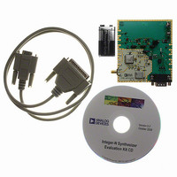
ADF4106 Evaluation Board
Manufacturer
Analog Devices Inc
Datasheet
1.ADF4106BCPZ.pdf
(24 pages)
Specifications of EVAL-ADF4106EBZ1
Silicon Manufacturer
Analog Devices
Application Sub Type
PLL Frequency Synthesizer
Kit Application Type
Clock & Timing
Silicon Core Number
ADF4106
Kit Contents
Board Including Synthesizer, Cables
Main Purpose
Timing, Frequency Synthesizer
Embedded
No
Utilized Ic / Part
ADF4106
Primary Attributes
Single Integer-N PLL
Secondary Attributes
6GHz, Graphical User Interface
Lead Free Status / RoHS Status
Lead free / RoHS Compliant


ADF4106
TABLE OF CONTENTS
Specifications ..................................................................................... 3
Absolute Maximum Ratings ............................................................ 5
Pin Configurations and Function Descriptions ........................... 6
Typical Performance Characteristics ............................................. 7
General Description ......................................................................... 9
REVISION HISTORY
2/10—Rev B to Rev. C
Changes to Figure 4 and Table 4 ..................................................... 6
Changes to Figure 12 ........................................................................ 8
Updated Outline Dimensions ....................................................... 20
Changes to Ordering Guide .......................................................... 21
6/05—Rev A to Rev. B
Updated Format .................................................................. Universal
Changes to Figure 1 .......................................................................... 1
Changes to Table 1 ............................................................................ 3
Changes to Table 2 ............................................................................ 4
Changes to Table 3 ............................................................................ 5
Changes to Figure 3 and Figure 4 ................................................... 6
Timing Characterisitics ............................................................... 4
ESD Caution .................................................................................. 5
Reference Input Section ............................................................... 9
RF Input Stage ............................................................................... 9
Prescaler (P/P +1) ......................................................................... 9
A Counter and B Counter ........................................................... 9
R Counter ...................................................................................... 9
Rev. C | Page 2 of 24
Applications ..................................................................................... 18
Outline Dimensions ....................................................................... 20
Changes to Figure 6 ........................................................................... 7
Changes to Figure 10 ......................................................................... 7
Deleted TPC 13 and TPC 14 ............................................................ 8
Changes to Figure 15 ......................................................................... 8
Changes to Figure 20 Caption ...................................................... 10
Updated Outline Dimensions ....................................................... 20
Changes to Ordering Guide .......................................................... 21
5/03—Rev 0 to Rev. A
Edits to Specifications ....................................................................... 2
Edits to TPC 11 .................................................................................. 7
Updated Outline Dimensions ....................................................... 19
10/01—Revision 0: Initial Revision
Phase Frequency Detector (PFD) and Charge Pump ............ 10
MUXOUT and Lock Detect ...................................................... 10
Input Shift Register .................................................................... 10
The Function Latch .................................................................... 16
The Initialization Latch ............................................................. 17
Local Oscillator for LMDS Base Station Transmitter ............ 18
Interfacing ................................................................................... 19
PCB Design Guidelines for Chip Scale Package .................... 19
Ordering Guide .......................................................................... 21
Related parts for EVAL-ADF4106EBZ1
Image
Part Number
Description
Manufacturer
Datasheet
Request
R

Part Number:
Description:
IC, ADJ LDO REG, 1.5V TO 5V 250mA MSOP-8
Manufacturer:
Vishay
Datasheet:

Part Number:
Description:
IC, ADJ LDO REG, 1.5V TO 5V 0.6A 8-TSSOP
Manufacturer:
Vishay
Datasheet:
Part Number:
Description:
IC, ADJ LDO REG, 1.5V TO 5V 250mA MSOP-8
Manufacturer:
Vishay
Datasheet:

Part Number:
Description:
IC ADJ LDO REG 1.5V TO 5V 150mA 5-SOT-23
Manufacturer:
Vishay
Datasheet:

Part Number:
Description:
BOARD EVAL AS1324-AD
Manufacturer:
austriamicrosystems
Datasheet:
Part Number:
Description:
IC, ADJ LDO REG, 1.5V TO 5V 0.6A 8-TSSOP
Manufacturer:
Vishay
Datasheet:

Part Number:
Description:
IC, ADJ LDO REG, 1.5V TO 5V, 0.3A, MSOP8
Manufacturer:
Vishay
Datasheet:
Part Number:
Description:
IC, ADJ LDO REG, 1.5V TO 5V, 0.3A, MSOP8
Manufacturer:
Vishay
Datasheet:
Part Number:
Description:
IC, ADJ LDO REG 1.215V TO 5V 0.3A MSOP-8
Manufacturer:
Vishay
Datasheet:
Part Number:
Description:
IC, ADJ LDO REG 1.215V TO 5V 0.3A MSOP-8
Manufacturer:
Vishay
Datasheet:

Part Number:
Description:
±1.7g Dual-Axis IMEMS Accelerometer Evaluation Board
Manufacturer:
Analog Devices Inc
Datasheet:

Part Number:
Description:
IC MULTIPLIER ANALOG 8-SOIC T/R
Manufacturer:
Analog Devices Inc
Datasheet:

Part Number:
Description:
IC ANALOG MULTIPLIER 8-DIP
Manufacturer:
Analog Devices Inc
Datasheet:
Part Number:
Description:
IC ANALOG MULTIPLIER 8-SOIC
Manufacturer:
Analog Devices Inc
Datasheet:
Part Number:
Description:
IC ANALOG MULTIPLIER 8-DIP
Manufacturer:
Analog Devices Inc
Datasheet: