EVAL-ADF4106EBZ1 Analog Devices Inc, EVAL-ADF4106EBZ1 Datasheet - Page 10
EVAL-ADF4106EBZ1
Manufacturer Part Number
EVAL-ADF4106EBZ1
Description
ADF4106 Evaluation Board
Manufacturer
Analog Devices Inc
Datasheet
1.ADF4106BCPZ.pdf
(24 pages)
Specifications of EVAL-ADF4106EBZ1
Silicon Manufacturer
Analog Devices
Application Sub Type
PLL Frequency Synthesizer
Kit Application Type
Clock & Timing
Silicon Core Number
ADF4106
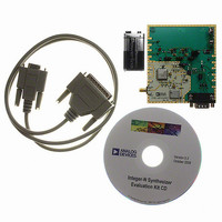
Kit Contents
Board Including Synthesizer, Cables
Main Purpose
Timing, Frequency Synthesizer
Embedded
No
Utilized Ic / Part
ADF4106
Primary Attributes
Single Integer-N PLL
Secondary Attributes
6GHz, Graphical User Interface
Lead Free Status / RoHS Status
Lead free / RoHS Compliant


ADF4106
PHASE FREQUENCY DETECTOR (PFD) AND
CHARGE PUMP
The PFD takes inputs from the R counter and N counter
(N = BP + A) and produces an output proportional to the
phase and frequency difference between them. Figure 20 is a
simplified schematic. The PFD includes a programmable delay
element that controls the width of the antibacklash pulse. This
pulse ensures that there is no dead zone in the PFD transfer
function and minimizes phase noise and reference spurs. Two
bits in the reference counter latch, ABP2 and ABP1, control the
width of the pulse. See Table 7.
MUXOUT AND LOCK DETECT
The output multiplexer on the ADF4106 allows the user
to access various internal points on the chip. The state of
MUXOUT is controlled by M3, M2, and M1 in the function
latch. Table 9 shows the full truth table. Figure 21 shows the
MUXOUT section in block diagram form.
Lock Detect
MUXOUT can be programmed for two types of lock detect:
digital lock detect and analog lock detect.
Digital lock detect is active high. When LDP in the R counter
latch is set to 0, digital lock detect is set high when the phase
error on three consecutive phase detector cycles is less than
15 ns. With LDP set to 1, five consecutive cycles of less than
15 ns are required to set the lock detect. It stays set high until a
phase error of greater than 25 ns is detected on any subsequent
PD cycle.
R DIVIDER
N DIVIDER
HI
HI
D2
D1
CLR2
CLR1
Figure 20. PFD Simplified Schematic
U1
U2
Q1
Q2
PROGRAMMABLE
UP
DOWN
ABP2
DELAY
ABP1
U3
CPGND
V
P
CHARGE
PUMP
Rev. C | Page 10 of 24
CP
The N-channel, open-drain, analog lock detect should be
operated with an external pull-up resistor of 10 kΩ nominal.
When lock is detected, this output is high with narrow, low-
going pulses.
ANALOG LOCK DETECT
INPUT SHIFT REGISTER
The ADF4106 digital section includes a 24-bit input shift
register, a 14-bit R counter, and a 19-bit N counter, comprising a
6-bit A counter and a 13-bit B counter. Data is clocked into the
24-bit shift register on each rising edge of CLK. The data is
clocked in MSB first. Data is transferred from the shift register
to one of four latches on the rising edge of LE. The destination
latch is determined by the state of the two control bits (C2, C1)
in the shift register. These are the two LSBs, DB1 and DB0, as
shown in the timing diagram of Figure 2. The truth table for
these bits is shown in Table 5. Table 6 shows a summary of how
the latches are programmed.
Table 5. C1, C2 Truth Table
Control Bits
C2
0
0
1
1
DIGITAL LOCK DETECT
R COUNTER OUTPUT
N COUNTER OUTPUT
C1
0
1
0
1
SDOUT
Data Latch
R Counter
N Counter (A and B)
Function Latch (Including Prescaler)
Initialization Latch
Figure 21. MUXOUT Circuit
MUX
CONTROL
DGND
DV
DD
MUXOUT
Related parts for EVAL-ADF4106EBZ1
Image
Part Number
Description
Manufacturer
Datasheet
Request
R

Part Number:
Description:
IC, ADJ LDO REG, 1.5V TO 5V 250mA MSOP-8
Manufacturer:
Vishay
Datasheet:

Part Number:
Description:
IC, ADJ LDO REG, 1.5V TO 5V 0.6A 8-TSSOP
Manufacturer:
Vishay
Datasheet:
Part Number:
Description:
IC, ADJ LDO REG, 1.5V TO 5V 250mA MSOP-8
Manufacturer:
Vishay
Datasheet:

Part Number:
Description:
IC ADJ LDO REG 1.5V TO 5V 150mA 5-SOT-23
Manufacturer:
Vishay
Datasheet:

Part Number:
Description:
BOARD EVAL AS1324-AD
Manufacturer:
austriamicrosystems
Datasheet:
Part Number:
Description:
IC, ADJ LDO REG, 1.5V TO 5V 0.6A 8-TSSOP
Manufacturer:
Vishay
Datasheet:

Part Number:
Description:
IC, ADJ LDO REG, 1.5V TO 5V, 0.3A, MSOP8
Manufacturer:
Vishay
Datasheet:
Part Number:
Description:
IC, ADJ LDO REG, 1.5V TO 5V, 0.3A, MSOP8
Manufacturer:
Vishay
Datasheet:
Part Number:
Description:
IC, ADJ LDO REG 1.215V TO 5V 0.3A MSOP-8
Manufacturer:
Vishay
Datasheet:
Part Number:
Description:
IC, ADJ LDO REG 1.215V TO 5V 0.3A MSOP-8
Manufacturer:
Vishay
Datasheet:

Part Number:
Description:
±1.7g Dual-Axis IMEMS Accelerometer Evaluation Board
Manufacturer:
Analog Devices Inc
Datasheet:

Part Number:
Description:
IC MULTIPLIER ANALOG 8-SOIC T/R
Manufacturer:
Analog Devices Inc
Datasheet:

Part Number:
Description:
IC ANALOG MULTIPLIER 8-DIP
Manufacturer:
Analog Devices Inc
Datasheet:
Part Number:
Description:
IC ANALOG MULTIPLIER 8-SOIC
Manufacturer:
Analog Devices Inc
Datasheet:
Part Number:
Description:
IC ANALOG MULTIPLIER 8-DIP
Manufacturer:
Analog Devices Inc
Datasheet: