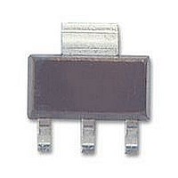
BSP171PL6327 Infineon Technologies, BSP171PL6327 Datasheet

BSP171PL6327
Specifications of BSP171PL6327
Related parts for BSP171PL6327
BSP171PL6327 Summary of contents
Page 1
SIPMOS ® Small-Signal-Transistor Features • P-Channel • Enhancement mode • Logic level • Avalanche rated • dv /dt rated • Pb-free lead plating; RoHS compliant Type Package BSP 171 P PG-SOT-223 Maximum ratings =25 °C, unless otherwise specified ...
Page 2
Parameter Thermal characteristics Thermal resistance, junction - soldering point Thermal resistance, junction - ambient Electrical characteristics Static characteristics Drain-source breakdown voltage Gate threshold voltage Zero gate voltage drain current Gate-source leakage current Drain-source on-state resistance Transconductance 1) Device ...
Page 3
Parameter Dynamic characteristics Input capacitance Output capacitance Reverse transfer capacitance Turn-on delay time Rise time Turn-off delay time Fall time 2) Gate Charge Characteristics Gate to source charge Gate to drain charge Gate charge total Gate plateau voltage Output charge ...
Page 4
Power dissipation P =f(T ) tot A 2 1 [° Safe operating area =25 ° parameter ...
Page 5
Typ. output characteristics I =f =25 ° parameter -4 Typ. transfer characteristics I ...
Page 6
Drain-source on-state resistance R =f =-1 =-10 V DS(on 500 400 98 % 300 200 typ. 100 0 -60 - [° Typ. capacitances C =f ...
Page 7
Avalanche characteristics parameter: T j(start 0 [µ Drain-source breakdown voltage V =f =-1 mA BR(DSS ...
Page 8
Package Outline SOT-223: Outline Footprint Dimensions in mm Rev 2.3 Packaging Tape page 8 BSP171P 2005-11-29 ...
Page 9
... Due to technical requirements, components may contain dangerous substances. For information on the types in question, please contact your nearest Infineon Technologies office. Infineon Technologies' components may only be used in life-support devices or systems with the expressed written approval of Infineon Technologies if a failure of such components can reasonably be expected to cause the failure of that life-support device or system affect the safety or effectiveness of that device or system ...


