SCR1100-D04 VTI Technologies, SCR1100-D04 Datasheet - Page 9
SCR1100-D04
Manufacturer Part Number
SCR1100-D04
Description
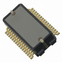
SENSOR GYRO 300DEG SNGL AXIS SPI
Manufacturer
VTI Technologies
Datasheet
1.SCR1100-D04.pdf
(21 pages)
Specifications of SCR1100-D04
New! Us2012 Catalog Page
Single Axis Gyroscopes
Range °/s
±300°/s
Sensitivity
18LSB/°/s
Typical Bandwidth
50Hz
Voltage - Supply
3 V ~ 3.6 V, 4.75 V ~ 5.25 V
Current - Supply
20mA, 26mA
Output Type
Analog, Digital
Operating Temperature
-40°C ~ 125°C
Package / Case
32-SOP
Lead Free Status / RoHS Status
Lead free / RoHS Compliant
Other names
551-1077-2


Address Transfer:
Data Transfer:
Status Flags:
VTI Technologies Oy
www.vti.fi
D15
0
D15
Dat14
D15
D14
0
D14
D14
Dat13
D13
0
D13
After the falling edge of CSN_G the device interprets the first 16-bit word is an address transfer
having a bit coding scheme below.
ADR[6:0] :
RW :
par odd :
The address selects an internal register of the device; the RW bit selects the access mode.
RW = ‘0'
transmission of the next word, the slave sends the requested register value to MISO_G. The slave
interprets the next word at MOSI_G as an address transfer.
RW = ‘1'
next transmitted word in the selected device register of MOSI_G and sends the actual register
value in response to MOSI_G. The transmission goes on with an address transfer to MOSI_G and
the address mode flags to MISO_G.
If the device is addressed by a nonexistent address it will respond with ´0´.
The next table shows the encoding scheme of a data value for a write access.
dat[14:0] :
par odd :
It is possible to combine the two access modes (write and read access) during one communication.
The communication can be finished after last transmitted word of mixed access communication
frame with CSN_G='1'. CSN_G must be '0' during mixed access communication frame.
SPI result values on MISO_G
Within SPI communication SCR1100 gyro ASIC sends Status Flags (Status/Config register value)
and register result values on MISO_G. The following two tables show the encoding scheme:
S_OK is generated out of the monitoring flags in the status register (08h).
D13
Dat12
D12
0
D12
D12
Dat11
D11
0
D11
Register address
RW=1 : Write access
RW=0 : Read access
odd parity bit.
par odd = 0 : the number of ones in the data word (D15:D1) is odd.
par odd = 1 : the number of ones in the data word (D15:D1) is even.
The master performs a read access on the selected register. During the
The master performs a write access on the selected register. The slave stores the
data value for write access (15 Bit)
see Address Transfer
D10
0
D10
D11
Dat10
Doc.Nr. 82 1226 00 A
Subject to changes
D9
ADR6
D9
D10
Dat9
D8
D8
ADR5
D9
Dat8
D7
D8
Dat7
D7
ADR4
D6
D7
Dat6
D6
ADR3
D5
D6
Dat5
D4
D5
ADR2
D5
Dat4
D3
D4
ADR1
Dat3
D4
D2
D3
Dat2
D3
ADR0
D1
s_ok
D2
Dat1
D2
RW
D1
Dat0
D0
par odd
0
D1
SCR1100-D04
D0
Par
odd
D0
Par
odd
Rev. 0.3
9/21
Related parts for SCR1100-D04
Image
Part Number
Description
Manufacturer
Datasheet
Request
R

Part Number:
Description:
Manufacturer:
Samtec Inc
Datasheet:
Part Number:
Description:
Manufacturer:
Samtec Inc
Datasheet:
Part Number:
Description:
SEALED CIRCULAR POWER RECEPTACLE
Manufacturer:
Samtec Inc

Part Number:
Description:
ACCELEROMETER SGL 1.7G DIL8 SMD
Manufacturer:
VTI Technologies
Datasheet:

Part Number:
Description:
VTI Automotive Digital Accelerometer Platform
Manufacturer:
VTI [VTI technologies]
Datasheet:

Part Number:
Description:
BOARD PWB ACCEL 3-AXIS SPI/I2C
Manufacturer:
VTI Technologies
Datasheet:

Part Number:
Description:
EVAL BOARD ACCELEROMETER Y-AXIS
Manufacturer:
VTI Technologies
Datasheet:

Part Number:
Description:
EVAL BOARD INCLINOMETER Y-AXIS
Manufacturer:
VTI Technologies
Datasheet:
Part Number:
Description:
ACCELEROMETER SGL 1.7G DIL8 SMD
Manufacturer:
VTI Technologies
Datasheet:
Part Number:
Description:
VTI Automotive Digital Accelerometer Platform
Manufacturer:
VTI [VTI technologies]
Datasheet:
Part Number:
Description:
Accelerometer
Manufacturer:
VTI [VTI technologies]
Datasheet:
Part Number:
Description:
Stand Alone Inclinometer
Manufacturer:
VTI [VTI technologies]
Datasheet:
Part Number:
Description:
3-axis accelerometer
Manufacturer:
VTI [VTI technologies]
Datasheet: