SCR1100-D04 VTI Technologies, SCR1100-D04 Datasheet - Page 2
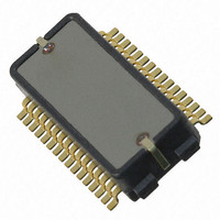
SCR1100-D04
Manufacturer Part Number
SCR1100-D04
Description
SENSOR GYRO 300DEG SNGL AXIS SPI
Manufacturer
VTI Technologies
Datasheet
1.SCR1100-D04.pdf
(21 pages)
Specifications of SCR1100-D04
New! Us2012 Catalog Page
Single Axis Gyroscopes
Range °/s
±300°/s
Sensitivity
18LSB/°/s
Typical Bandwidth
50Hz
Voltage - Supply
3 V ~ 3.6 V, 4.75 V ~ 5.25 V
Current - Supply
20mA, 26mA
Output Type
Analog, Digital
Operating Temperature
-40°C ~ 125°C
Package / Case
32-SOP
Lead Free Status / RoHS Status
Lead free / RoHS Compliant
Other names
551-1077-2


1 General Description .........................................................................................3
2 Specifications...................................................................................................5
3 Reset and Power Up ........................................................................................8
4 Component Interfacing ....................................................................................8
5 Contact Information .......................................................................................21
VTI Technologies Oy
www.vti.fi
TABLE OF CONTENTS
1.1
1.2
1.3
2.1
2.2
2.3
2.4
3.1
3.2
4.1
4.2
4.3
4.4
4.5
4.6
4.7
4.8
1.2.1
4.1.1
4.1.2
4.2.1
4.2.2
4.2.3
4.4.1
4.5.1
4.5.2
4.7.1
4.7.2
Introduction ..................................................................................................................................3
General Product Description ......................................................................................................3
Abbreviations ...............................................................................................................................4
Performance Specifications for Gyroscope ..............................................................................5
Absolute Maximum Ratings........................................................................................................6
Digital I/O Specification...............................................................................................................6
SPI AC Characteristics ................................................................................................................7
Power-up Sequence.....................................................................................................................8
Reset .............................................................................................................................................8
SPI Interfaces ...............................................................................................................................8
ASIC Addressing Space ............................................................................................................11
Pin Description...........................................................................................................................13
Application Circuitry and External Component Characteristics ...........................................14
Boost Regulator and Power Supply Decoupling in Layout ...................................................16
Measurement Axis and Directions ...........................................................................................18
Package Characteristics ...........................................................................................................19
Assembly instructions ..............................................................................................................20
Factory Calibration................................................................................................................4
SPI Transfer ...........................................................................................................................8
SPI Transfer Parity Mode....................................................................................................10
Register Definition ..............................................................................................................11
Data Register Block ............................................................................................................11
Temperature Output Registers ..........................................................................................12
Separate Analog and Digital Ground Layers with Long Power Supply Lines ...............15
Layout Example...................................................................................................................17
Thermal Connection............................................................................................................17
Package Outline Drawing ...................................................................................................19
PCB Footprint ......................................................................................................................20
Doc.Nr. 82 1226 00 A
Subject to changes
SCR1100-D04
Rev. 0.3
2/21
Related parts for SCR1100-D04
Image
Part Number
Description
Manufacturer
Datasheet
Request
R

Part Number:
Description:
Manufacturer:
Samtec Inc
Datasheet:
Part Number:
Description:
Manufacturer:
Samtec Inc
Datasheet:
Part Number:
Description:
SEALED CIRCULAR POWER RECEPTACLE
Manufacturer:
Samtec Inc

Part Number:
Description:
ACCELEROMETER SGL 1.7G DIL8 SMD
Manufacturer:
VTI Technologies
Datasheet:

Part Number:
Description:
VTI Automotive Digital Accelerometer Platform
Manufacturer:
VTI [VTI technologies]
Datasheet:

Part Number:
Description:
BOARD PWB ACCEL 3-AXIS SPI/I2C
Manufacturer:
VTI Technologies
Datasheet:

Part Number:
Description:
EVAL BOARD ACCELEROMETER Y-AXIS
Manufacturer:
VTI Technologies
Datasheet:

Part Number:
Description:
EVAL BOARD INCLINOMETER Y-AXIS
Manufacturer:
VTI Technologies
Datasheet:
Part Number:
Description:
ACCELEROMETER SGL 1.7G DIL8 SMD
Manufacturer:
VTI Technologies
Datasheet:
Part Number:
Description:
VTI Automotive Digital Accelerometer Platform
Manufacturer:
VTI [VTI technologies]
Datasheet:
Part Number:
Description:
Accelerometer
Manufacturer:
VTI [VTI technologies]
Datasheet:
Part Number:
Description:
Stand Alone Inclinometer
Manufacturer:
VTI [VTI technologies]
Datasheet:
Part Number:
Description:
3-axis accelerometer
Manufacturer:
VTI [VTI technologies]
Datasheet: