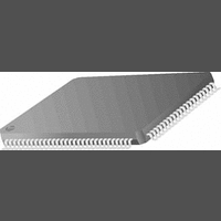
DS90C387VJD National Semiconductor, DS90C387VJD Datasheet - Page 6

DS90C387VJD
Manufacturer Part Number
DS90C387VJD
Description
Transceiver IC
Manufacturer
National Semiconductor
Datasheet
1.DS90C387VJD.pdf
(26 pages)
Specifications of DS90C387VJD
No. Of Drivers
2
Driver Case Style
TQFP
No. Of Pins
100
Transceiver Type
Display Interface
Mounting Type
Surface Mount
No. Of Channels
8
No. Of Driver/receivers
2/2
Peak Reflow Compatible (260 C)
No
Lead Free Status / RoHS Status
Contains lead / RoHS non-compliant
Available stocks
Company
Part Number
Manufacturer
Quantity
Price
Company:
Part Number:
DS90C387VJD
Manufacturer:
DIODES
Quantity:
12 000
Company:
Part Number:
DS90C387VJD
Manufacturer:
Texas Instruments
Quantity:
10 000
Company:
Part Number:
DS90C387VJD/NOPB
Manufacturer:
TI
Quantity:
1 000
Company:
Part Number:
DS90C387VJD/NOPB
Manufacturer:
Texas Instruments
Quantity:
10 000
Company:
Part Number:
DS90C387VJDX/NOPB
Manufacturer:
TI
Quantity:
1 000
Company:
Part Number:
DS90C387VJDX/NOPB
Manufacturer:
Texas Instruments
Quantity:
10 000
www.national.com
Symbol
RPLLS
RPDD
RSKM
RSKM
RSKMD
RDR
RDSS
Symbol
Receiver Switching Characteristics
Over recommended operating supply and temperature ranges unless otherwise specified.
Chipset RSKM Characteristics
Over recommended operating supply and temperature ranges unless otherwise specified.(Notes 4, 8). See Applications Infor-
mation section for more details on this parameter and how to apply it.
Note 4: The Minimum and Maximum Limits are based on statistical analysis of the device performance over voltage and temperature ranges. This parameter is
functionally tested on Automatic Test Equipment (ATE). ATE is limited to 85MHz. A sample of characterization parts have been bench tested to verify functional
performance.
Note 5: The limits are based on bench characterization of the device’s jitter response over the power supply voltage range. Output clock jitter is measured with a
cycle-to-cycle jitter of
in the clock edge from most graphics VGA chips currently available. This parameter is used when calculating system margin as described in AN-1059.
Note 6: Receiver Skew Margin (RSKM) is defined as the valid data sampling region at the receiver inputs. This margin takes into account transmitter output pulse
positions (min and max) and the receiver input setup and hold time (internal data sampling window - RSPOS). This margin allows for LVDS interconnect skew,
inter-symbol interference (both dependent on type/length of cable) and clock jitter.
RSKM ≥ cable skew (type, length) + source clock jitter (cycle to cycle, TJCC) + ISI (if any). See Applications Information section for more details.
Note 7: Receiver Skew Margin with Deskew (RSKMD) is defined as the valid data sampling region at the receiver inputs. The DESKEW function will constrain the
receiver’s sampling strobes to the middle half of the LVDS bit and removes (adjusts for) fixed interconnect skew. This margin (RSKMD) allows for inter-symbol
interference (dependent on type/length of cable), Transmitter Pulse Position (TPPOS) variance, and LVDS clock jitter (TJCC).
RSKMD ≥ ISI + TPPOS(variance) + source clock jitter (cycle to cycle). See Applications Information section for more details.
Note 8: Typical values for RSKM and RSKMD are applicable for fixed V
T
A
points).
Receiver Phase Lock Loop Set (Figure 9)
Receiver Powerdown Delay (Figure 11)
Receiver Skew Margin without
Deskew in non-DC Balance Mode,
(Figure 12), (Note 6)
Receiver Skew Margin without
Deskew in DC Balance Mode,
(Figure 12), (Note 6)
Receiver Skew Margin with Deskew
in DC Balance, (Figure 13),
(Note 7)
Receiver Deskew Range
Receiver Deskew Step Size
±
3ns applied to the input clock signal while data inputs are switching (see figures 15 and 16). A jitter event of 3ns, represents worse case jump
Parameter
Parameter
f = 112 MHz
f = 100 MHz
f = 85MHz
f = 66MHz
f = 112 MHz
f = 100 MHz
f = 85 MHz
f = 66 MHz
f = 50MHz
f = 40MHz
f = 40 to 80
MHz
f = 80 MHz
f = 80 MHz
CC
and T
(Continued)
6
A
for the Transmitter and Receiver (both are assumed to be at the same V
0.25TBIT
Min
170
170
300
300
170
170
250
250
100
±
94
1
Min
0.3 TBIT
Typ
240
350
350
200
300
300
350
530
Typ
Max
Max
10
1
Units
CC
ms
Units
µs
TBIT
ps
ps
ps
ps
ps
ps
ps
ps
ps
ps
ps
ns
and


