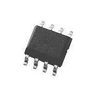
LP2975AIMM-5.0 National Semiconductor, LP2975AIMM-5.0 Datasheet - Page 19

LP2975AIMM-5.0
Manufacturer Part Number
LP2975AIMM-5.0
Description
IC, LDO VOLT REG, 5V, 5A, 8-SOIC
Manufacturer
National Semiconductor
Datasheet
1.LP2975IMM-5.0NOPB.pdf
(20 pages)
Specifications of LP2975AIMM-5.0
Primary Input Voltage
24V
Output Voltage Fixed
5V
Dropout Voltage Vdo
323mV
No. Of Pins
8
Output Current
5A
Operating Temperature Range
-40°C To +125°C
Device Type
LDO
Termination Type
SMD
Lead Free Status / RoHS Status
Contains lead / RoHS non-compliant
Available stocks
Company
Part Number
Manufacturer
Quantity
Price
Company:
Part Number:
LP2975AIMM-5.0
Manufacturer:
NSC
Quantity:
800
Company:
Part Number:
LP2975AIMM-5.0
Manufacturer:
NS
Quantity:
100
Company:
Part Number:
LP2975AIMM-5.0
Manufacturer:
MIT
Quantity:
6 218
Part Number:
LP2975AIMM-5.0
Manufacturer:
NS/国半
Quantity:
20 000
Application Hints
LOW OUTPUT VOLTAGE AND C
The feed-forward capacitor C
shift (lead) which can be used to cancel some of the excess
phase lag from any of the various poles present in the loop.
However, it is important to note that the effectiveness of C
decreases with output voltage.
This is due to the fact that the frequencies of the zero f
pole f
(see equations in section FEED-FORWARD COMPENSA-
TION).
C
apart, because there is less self cancellation. The net benefit
in phase shift provided by C
lead (positive phase shift) from f
phase shift) from f
quency f
other, that difference diminishes to nothing.
The amount of phase lead at f
both on the f
To illustrate this more clearly, a graph is provided which
shows how much phase lead can be obtained for V
12V, 5V, and 3.3V (see graph PHASE LEAD PROVIDED BY
C
The most important information on the graph is the fre-
quency range of f
(most positive phase shift):
For V
For V
For V
It’s also important to note how the maximum available phase
shift that C
than 50˚ can be obtained, but at 3.3V less than 30˚ is
possible. The lesson from this is that higher voltage designs
are more tolerant of phase shifts from both f
capacitance pole) and incorrect placement of f
F
F
).
is more effective when the pole-zero pair are farther
pf
OUT
OUT
OUT
get closer together as the output voltage is reduced
c
. As the pole and zero frequency approach each
= 12V: 0.1 f
= 5V: 0.2 f
= 3.3V: 0.2 f
F
zf/
can provide drops off with V
f
pf
Phase Lead Provided by C
ratio and the location of f
zf
pf
which will provide the maximum benefit
c
which is present at the crossover fre-
c
<
c
<
<
f
z
f
z
f
<
z
F
<
<
F
1.2 f
is the difference between the
1.0 f
will provide a positive phase
1.3 f
(Continued)
C
c
F
provided by C
zf
c
c
and the lag (negative
z
OUT
with respect to f
F
. At 12V, more
10003433
pg
F
(the gate
z
depends
(which
OUT
zf
and
c
=
F
.
19
means the output capacitor ESR is not at its nominal value).
At lower values of V
precisely selected since C
tion.
GENERAL DESIGN PROCEDURE
Assuming that V
1) Calculate the required value of capacitance for C
that the pole f
CAPACITOR). For this calculation, an ESR of about 0.1Ω
can be assumed for the purpose of determining C
IMPORTANT: If a smaller value of output capacitor is used
(so that the value of f
control loop will be reduced. This will result in increased
ringing on the output voltage during a load transient. If the
output capacitor is made extremely small, oscillations will
result.
To illustrate this effect, scope photos have been presented
showing the output voltage of reference design #2 as the
output capacitor is reduced to approximately 1/30 of the
nominal value (the value which sets f
the effect of deviating from the nominal value is gradual and
the regulator is quite robust in resisting going into oscilla-
tions.
2) Approximate the crossover frequency f
tion in the previous section CROSSOVER FREQUENCY
AND PHASE MARGIN.
3) Calculate the required ESR of the output capacitor so that
the frequency of the zero f
section OUTPUT CAPACITOR).
4) Calculate the value of the feed-forward capacitor C
that the zero f
maximum phase gain for the output voltage selected (see
previous section LOW OUTPUT VOLTAGE AND C
formula for calculating C
FORWARD CAPACITOR.
Lower ESR electrolytics are available which use organic
electrolyte (OSCON types), but are more costly than typical
aluminum electrolytics.
If the calculated value of ESR is higher than what is found in
the selected capacitor, an external resistor can be placed in
series with C
LOW VOLTAGE DESIGNS: Designs which have a low out-
put voltage (where the positive effects of C
may be marginally stable if the C
carefully selected.
Also, if the FET gate capacitance is large (as in the case of
a high-current FET), the pole f
enough in frequency to cause a problem.
The solution in both cases is to increase the amount of
output capacitance which will shift f
(and reduce overall loop bandwidth). The ESR and C
culations should be repeated, since this changes the cross-
over frequency f
OUT
p
zf
c
IN
≤ 200 Hz (see previous section OUTPUT
.
.
occurs at the frequency which yields the
, V
OUT
OUT
p
>
F
, these parameters must be more
, and R
200 Hz), the phase margin of the
F
is in the previous section FEED-
can not provide as much correc-
z
is set to 0.5 f
OUT
L
pg
are defined:
could possibly get low
and ESR values are not
p
p
= 200 Hz). As shown,
to a lower frequency
c
F
using the equa-
c
are very small)
(see previous
www.national.com
OUT
F
OUT
). The
.
F
F
cal-
so
so


