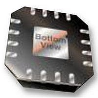
ADP322ACPZ-155 Analog Devices Inc, ADP322ACPZ-155 Datasheet - Page 4

ADP322ACPZ-155
Manufacturer Part Number
ADP322ACPZ-155
Description
IC, LDO, TRIPLE, 0.2A, 16LFCSP
Manufacturer
Analog Devices Inc
Datasheet
1.ADP322ACPZ-175-R7.pdf
(24 pages)
Specifications of ADP322ACPZ-155
Primary Input Voltage
3.8V
Output Voltage
3.3V
Dropout Voltage Vdo
110mV
No. Of Pins
16
Output Current
200mA
Voltage Regulator Case Style
LFCSP
Operating Temperature Range
-40°C To +125°C
Output Voltage Fixed
3.3V
Rohs Compliant
Yes
Lead Free Status / RoHS Status
Lead free / RoHS Compliant
ADP322/ADP323
Parameter
EN INPUT
UNDERVOLTAGE LOCKOUT
OUTPUT NOISE
POWER SUPPLY REJECTION RATIO
1
2
3
4
5
INPUT AND OUTPUT CAPACITOR, RECOMMENDED SPECIFICATIONS
Table 2.
Parameter
MINIMUM INPUT AND OUTPUT CAPACITANCE
CAPACITOR ESR
1
Accuracy when VOUTx is connected directly to FBx. When the VOUTx voltage is set by external feedback resistors, the absolute accuracy in adjust mode depends on
the tolerances of the resistors used.
Based on an end-point calculation using 1 mA and 200 mA loads.
The dropout voltage specification applies only to output voltages greater than 1.8 V. Dropout voltage is defined as the input-to-output voltage differential when the
input voltage is set to the nominal output voltage.
Start-up time is defined as the time between the rising edge of ENx to VOUTx being at 90% of its nominal value.
Current-limit threshold is defined as the current at which the output voltage drops to 90% of the specified typical value. For example, the current limit for a 3.0 V
output voltage is defined as the current that causes the output voltage to drop to 90% of 3.0 V, that is, 2.7 V.
The minimum input and output capacitance should be greater than 0.70 µF over the full range of operating conditions. The full range of operating conditions in the
application must be considered during device selection to ensure that the minimum capacitance specification is met. X7R and X5R type capacitors are recommended;
Y5V and Z5U capacitors are not recommended for use with LDOs.
EN Input Logic High
EN Input Logic Low
EN Input Leakage Current
Input Bias Voltage (VBIAS)
Input Bias Voltage (VBIAS)
Hysteresis
Rising
Falling
Symbol
V
V
V
UVLO
UVLO
UVLO
UVLO
OUT
PSRR
IH
IL
I-LEAKAGE
NOISE
RISE
FALL
HYS
1
Conditions
2.5 V ≤ V
2.5 V ≤ V
EN1 = EN2 = EN3 = V
EN1 = EN2 = EN3 = V
T
10 Hz to 100 kHz, V
10 Hz to 100 kHz, V
10 Hz to 100 kHz, V
10 Hz to 100 kHz, V
V
100 Hz
1 kHz
10 kHz
100 kHz
1 MHz
V
100 Hz
1 kHz
10 kHz
100 kHz
1 MHz
J
IN
IN
= −40°C to +125°C
= 1.8 V, V
= 3.8 V, V
Symbol
C
R
BIAS
BIAS
Rev. 0 | Page 4 of 24
ESR
MIN
≤ 5.5 V
≤ 5.5 V
OUT
OUT
= 0.8 V, I
= 2.8 V, I
IN
IN
IN
IN
IN
IN
= 5 V, V
= 5 V, V
= 3.6 V, V
= 3.6 V, V
Conditions
T
T
or GND
or GND,
A
A
OUT
OUT
= −40°C to +125°C
= −40°C to +125°C
= 100 mA
= 100 mA
OUT
OUT
OUT
OUT
= 3.3 V
= 2.8 V
= 2.5 V
= 1.2 V
Min
0.70
0.001
Min
1.2
2.0
Typ
Typ
0.1
180
63
55
50
29
70
70
70
60
40
68
62
68
60
40
Max
0.4
1
2.45
Max
1
Unit
V
V
µA
µA
V
V
mV
µV rms
µV rms
µV rms
µV rms
dB
dB
dB
dB
dB
dB
dB
dB
dB
dB
Unit
µF
Ω


