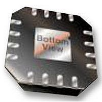
ADP322ACPZ-145 Analog Devices Inc, ADP322ACPZ-145 Datasheet - Page 16

ADP322ACPZ-145
Manufacturer Part Number
ADP322ACPZ-145
Description
IC, LDO, TRIPLE, 0.2A, 16LFCSP
Manufacturer
Analog Devices Inc
Datasheet
1.ADP322ACPZ-175-R7.pdf
(24 pages)
Specifications of ADP322ACPZ-145
Primary Input Voltage
3.8V
Output Voltage
3.3V
Dropout Voltage Vdo
110mV
No. Of Pins
16
Output Current
200mA
Voltage Regulator Case Style
LFCSP
Operating Temperature Range
-40°C To +125°C
Output Voltage Fixed
3.3V
Rohs Compliant
Yes
Lead Free Status / RoHS Status
Lead free / RoHS Compliant
ADP322/ADP323
APPLICATIONS INFORMATION
CAPACITOR SELECTION
Output Capacitor
The ADP322/ADP323 are designed for operation with small,
space-saving ceramic capacitors, but the parts function with
most commonly used capacitors as long as care is taken with
the effective series resistance (ESR) value. The ESR of the
output capacitor affects the stability of the LDO control loop.
A minimum of 0.70 µF capacitance with an ESR of 1 Ω or less is
recommended to ensure the stability of the ADP322/ADP323.
Transient response to changes in load current is also affected by
output capacitance. Using a larger value of output capacitance
improves the transient response of the ADP322/ADP323 to large
changes in the load current. Figure 45 shows the transient
response for an output capacitance value of 1 µF.
1
2
3
4
CH3 10mV
CH1
I
LOAD1
CH1 = I
100mA Ω
= 1 mA to 200 mA, I
Figure 45. Output Transient Response,
LOAD1
B
B
W
W
, CH2 = V
CH2 50mV
CH4 10mV
OUT1
I
V
V
V
LOAD1
OUT1
OUT2
OUT3
LOAD2
, CH3 = V
B
B
W
W
M40µs
= 1 mA, I
T
9.8%
OUT2
, CH4 = V
LOAD3
A CH1
= 1 mA,
OUT3
44mA
Rev. 0 | Page 16 of 24
Input Bypass Capacitor
Connecting a 1 µF capacitor from VIN1/VIN2, VIN3, and
VBIAS to GND reduces the circuit sensitivity to the PCB layout,
especially when long input traces or high source impedance is
encountered. If an output capacitance greater than 1 µF is
required, the input capacitor should be increased to match it.
Input and Output Capacitor Properties
Any good quality ceramic capacitor can be used with the ADP322/
ADP323, as long as the capacitor meets the minimum capacit-
ance and maximum ESR requirements. Ceramic capacitors are
manufactured with a variety of dielectrics, each with a different
behavior over temperature and applied voltage. Capacitors must
have an adequate dielectric to ensure the minimum capacitance
over the necessary temperature range and dc bias conditions.
X5R or X7R dielectrics with a voltage rating of 6.3 V or 10 V are
recommended. Y5V and Z5U dielectrics are not recommended
due to their poor temperature and dc bias characteristics.
Figure 46 depicts the capacitance vs. voltage bias characteristic
of a 0402 1 µF, 10 V, X5R capacitor. The voltage stability of a
capacitor is strongly influenced by the capacitor size and voltage
rating. In general, a capacitor in a larger package or with a higher
voltage rating exhibits better stability. The temperature variation
of the X5R dielectric is about ±15% over the −40°C to +85°C
temperature range and is not a function of the package or
voltage rating.
1.2
1.0
0.8
0.6
0.4
0.2
0
0
Figure 46. Capacitance vs. Voltage Bias Characteristic
2
VOLTAGE (V)
4
6
8
10


