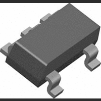
LM2611BMF National Semiconductor, LM2611BMF Datasheet - Page 6

LM2611BMF
Manufacturer Part Number
LM2611BMF
Description
IC, PWM INVERTING SWITCHING REG, SOT23-5
Manufacturer
National Semiconductor
Datasheet
1.LM2611AMFNOPB.pdf
(15 pages)
Specifications of LM2611BMF
Primary Input Voltage
5V
No. Of Outputs
1
Output Voltage
-36V
Output Current
1A
No. Of Pins
5
Operating Temperature Range
-40°C To +125°C
Supply Voltage Range
2.7V To 14V
Lead Free Status / RoHS Status
Contains lead / RoHS non-compliant
Available stocks
Company
Part Number
Manufacturer
Quantity
Price
Company:
Part Number:
LM2611BMF
Manufacturer:
NS
Quantity:
3 684
Company:
Part Number:
LM2611BMF
Manufacturer:
FAIRCHILD
Quantity:
1 469
Part Number:
LM2611BMF
Manufacturer:
NS/国半
Quantity:
20 000
Company:
Part Number:
LM2611BMFX
Manufacturer:
NS
Quantity:
5 321
Company:
Part Number:
LM2611BMFX
Manufacturer:
NS
Quantity:
21 534
Part Number:
LM2611BMFX
Manufacturer:
TI/德州仪器
Quantity:
20 000
www.national.com
Operation
Cuk Converter
The LM2611 is a current mode, fixed frequency PWM
switching regulator with a −1.23V reference that makes it
ideal for use in a Cuk converter. The Cuk converter inverts
the input and can step up or step down the absolute value.
Using inductors on both the input and output, the Cuk con-
verter produces very little input and output current ripple.
This is a significant advantage over other inverting topolo-
gies such as the buck-boost and flyback.
The operating states of the Cuk converter are shown in
Figure 1. During the first cycle, the transistor switch is closed
and the diode is open. L1 is charged by the source and L2 is
charged by C
In the second cycle, L1 charges C
through the load. By applying the volt-second balance to
either of the inductors, the relationship of V
cycle (D) is found to be:
The following sections review the steady-state design of the
LM2611 Cuk converter.
Output and Input Inductor
Figure 2 and Figure 3 show the steady-state voltage and
current waveforms for L1 and L2, respectively. Referring to
Figure 1 (a), when the switch is closed, V
L1. In the next cycle, the switch opens and the diode be-
comes forward biased, and V
voltage across C
CUK
CUK
, while the output current is provided by L2.
is V
IN
− V
OUT
OUT
is applied across L1 (the
.
CUK
FIGURE 1. Operating Cycles of a Cuk Converter
and L2 discharges
IN
is applied across
OUT
to the duty
6
The voltage and current waveforms of inductor L2 are shown
in Figure 3. During the first cycle of operation, when the
switch is closed, V
opens, V
FIGURE 2. Voltage and Current Waveforms in Inductor
FIGURE 3. Voltage and Current Waveforms in Inductor
OUT
is applied across L2.
L1 of a Cuk Converter
L2 of a Cuk Converter
IN
is applied across L2. When the switch
20018103
20018104
20018105


