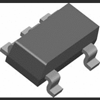
LM2611BMF National Semiconductor, LM2611BMF Datasheet

LM2611BMF
Specifications of LM2611BMF
Available stocks
Related parts for LM2611BMF
LM2611BMF Summary of contents
Page 1
... Grade A Current Limit 1.2A R 0.5Ω DS(ON) Typical Application Circuit © 2005 National Semiconductor Corporation Features n 1.4MHz switching frequency n Low R DS(ON) n 1mVp-p output ripple n −5V at 300mA from 5V input n Better regulation than a charge pump n Uses tiny capacitors and inductors n Wide input range: 2 ...
Page 2
... Connection Diagram Ordering Information Order Number Package Type LM2611AMF LM2611AMFX SOT23-5 LM2611BMF LM2611BMFX Pin Description Pin Name GND 3 NFB 4 SHDN Block Diagram www.national.com Top View 20018115 5-lead SOT-23 Package NS Package Number MF05A NSC Package Drawing MF05A Drain of internal switch. Connect at the node of the input inductor and Cuk capacitor. ...
Page 3
... Absolute Maximum Ratings If Military/Aerospace specified devices are required, please contact the National Semiconductor Sales Office/ Distributors for availability and specifications Voltage NFB Voltage SHDN Voltage Maximum Junction Temperature Power Dissipation (Note 2) Lead Temperature Electrical Characteristics Specifications in standard type face are for T − ...
Page 4
Typical Performance Characteristics DS(ON) Switch Current Limit vs. V Oscillator Frequency vs V www.national.com IN 20018112 Switch Current Limit vs Ambient Temperature IN 20018111 Oscillator Frequency vs Ambient Temperature IN 20018119 4 R Vs. Ambient Temperature DS(ON) ...
Page 5
Typical Performance Characteristics NFB 25˚ −5V A OUT NFB 25˚ −5V A OUT I vs Ambient Temperature (No Load) q (Continued Ambient ...
Page 6
Operation Cuk Converter The LM2611 is a current mode, fixed frequency PWM switching regulator with a −1.23V reference that makes it ideal for use in a Cuk converter. The Cuk converter inverts the input and can step up or step ...
Page 7
Operation (Continued) The following equations define values given in Figure 2 and Figure OUT Use these equations to choose correct core sizes for the inductors. The design of the LM2611’s internal compensa- tion assumes L1 ...
Page 8
Operation (Continued) The optimal position for this zero-pole pair will vary with circuit parameters such OUT For most cases, the value for the zero frequency is between 5 kHz to 20 kHz. Notice how the ...
Page 9
Operation (Continued) Thermal Shutdown If the junction temperature of the LM2611 exceeds 163˚C, it will enter thermal shutdown. In thermal shutdown, the part deactivates the driver and the switch turns off. The switch FIGURE 8. At low loads, the LM2611 ...
Page 10
Application Circuits Efficiency vs Load Current FIGURE 9. The Maximum Output Current vs Output Voltage (Adjust R www.national.com 5V to -5V Inverting Converter 20018158 to Set a Different Output Voltage) When The FB2 Input Voltage 20018117 20018160 ...
Page 11
Application Circuits (Continued -5V Inverting Converter FIGURE 10. The Maximum Output Current vs Output Voltage (Adjust R to Set a Different Output Voltage) FB2 When The Input Voltage is 9V 12V to -5V Inverting Converter 20018164 FIGURE 11. ...
Page 12
Application Circuits FIGURE 12. LM2611 Operating with Separate Power and Biasing Supplies Split Supply Operation The LM2611 may be operated with separate power and bias supplies. In the circuit shown in Figure 12. V supply that the regulated voltage is ...
Page 13
Application Circuits (Continued) FIGURE 14. Start-Up Waveforms with Soft Start Circuit FIGURE 15. Start-Up Waveforms without Soft Start Circuit FIGURE 13. LM2611 Soft Start Circuit 20018142 20018141 13 20018125 www.national.com ...
Page 14
Application Circuits High Duty Cycle/Load Current Operation The circuit in Figure 16 is used for high duty cycles (D and high load currents. The duty cycle will begin to increase beyond 50% as the input voltage drops below the absolute ...
Page 15
... BANNED SUBSTANCE COMPLIANCE National Semiconductor certifies that the products and packing materials meet the provisions of the Customer Products Stewardship Specification (CSP-9-111C2) and the Banned Substances and Materials of Interest Specification (CSP-9-111S2) and contain no ‘‘Banned Substances’’ as defined in CSP-9-111S2. ...


