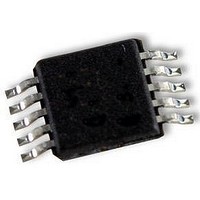
XC9223B081AR Torex Semiconductor Ltd, XC9223B081AR Datasheet - Page 9

XC9223B081AR
Manufacturer Part Number
XC9223B081AR
Description
BUCK CONVERTER, 1MHZ SYNC., 9223
Manufacturer
Torex Semiconductor Ltd
Datasheet
1.XC9223B081AR.pdf
(25 pages)
Specifications of XC9223B081AR
Primary Input Voltage
6V
No. Of Outputs
1
Output Voltage
6V
Output Current
1A
Voltage Regulator Case Style
MSOP
No. Of Pins
10
Operating Temperature Range
-40°C To +85°C
Svhc
No SVHC
Lead Free Status / RoHS Status
Lead free / RoHS Compliant
Available stocks
Company
Part Number
Manufacturer
Quantity
Price
Part Number:
XC9223B081AR
Manufacturer:
TOREX
Quantity:
20 000
■OPERATIONAL EXPLANATION
Each unit of the XC9223/XC9224 series consists of a reference voltage source, a ramp wave circuit, error amplifier, PWM
comparator, phase compensation circuit, output voltage adjustment resistors, P-channel MOS driver transistor, N-channel
MOS synchronous rectification switching transistor, current limiter circuit, U.V.L.O. circuit and others.
compares, using the error amplifier, the internal reference voltage to the V
R
comparator to determine the turn-on time during PWM operation. The PWM comparator compares, in terms of voltage
level, the signal from the error amplifier with the ramp wave from the ramp wave circuit, and delivers the resulting output to
the buffer driver circuit to cause the Lx pin to output a switching duty cycle. This process is continuously performed to
ensure stable output voltage. The current feedback circuit monitors the P-channel MOS driver transistor current for each
switching operation, and modulates the error amplifier output signal to provide multiple feedback signals. This enables a
stable feedback loop even when a low ESR capacitor, such as a ceramic capacitor, is used, ensuring stable output voltage.
<Reference Voltage Source>
The reference voltage source provides the reference voltage to ensure stable output voltage of the DC/DC converter.
The ramp wave circuit determines switching frequency. The frequency is fixed internally and can be selected from 1.0MHz
and 2.0MHz. Clock pulses generated in this circuit are used to produce ramp waveforms needed for PWM operation, and
to synchronize all the internal circuits.
<Current Limit>
The IC waits for the over current state to end by repeating the steps 1 through 3. If an over current state continues for
several msec and the above three steps are repeatedly performed, the IC performs the function of latching the OFF state of
the driver transistor, and goes into operation suspension mode. After being put into suspension mode, the IC can resume
operation by turning itself off once and then starting it up using the CE pin, or by restoring power to the V
latch time may be released from a current limit detection state because of the noise. Depending on the state of a substrate,
it may result in the case where the latch time may become longer or the operation may not be latched. Please locate an
input capacitor as close as possible.
<Error Amplifier>
The error amplifier is designed to monitor output voltage. The amplifier compares the reference voltage with the feedback
voltage divided by the internal resistors (R
output voltage of the error amplifier increases. The gain and frequency characteristics of the error amplifier output are
fixed internally to deliver an optimized signal to the mixer.
The current limiter circuit of the XC9223/XC9224 series monitors the current flowing through the P-channel MOS driver
transistor connected to the Lx pin, and features a combination of the constant-current type current limit mode and the
operation suspension mode. For the current limit values, please select the values either from 1.2A (MIN.) when the LIM
pin is high level or 0.6A (MIN.) when the LIM pin is low level.
<Ramp Wave Circuit>
FB1
1When the driver current is greater than a specific level, the constant-current type current limit function operates to turn
2When the driver transistor is turned off, the limiter circuit is then released from the current limit detection state.
3At the next pulse, the driver transistor is turned on. However, the transistor is immediately turned off in the case of an
4 When the over current state is eliminated, the IC resumes its normal operation.
off the pulses from the Lx pin at any given time.
over current state.
and R
VOUT
IOUT
VIN
CE
LX
FB2
. Phase compensation is performed on the resulting error amplifier output, to input a signal to the PWM
Limit < # mS
FB
1 and R
ms
FB2
). When a voltage lower than the reference voltage is fed back, the
Limit > # mS
ms
OUT
pin with the voltage feedback via resistors
Current Limit LEVEL
Restart
XC9223/XC9224
VSS
0mA
IN
pin. Integral
The series
Series
9/25


