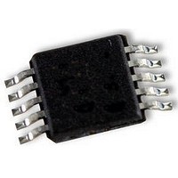
XC9223B081AR Torex Semiconductor Ltd, XC9223B081AR Datasheet - Page 8

XC9223B081AR
Manufacturer Part Number
XC9223B081AR
Description
BUCK CONVERTER, 1MHZ SYNC., 9223
Manufacturer
Torex Semiconductor Ltd
Datasheet
1.XC9223B081AR.pdf
(25 pages)
Specifications of XC9223B081AR
Primary Input Voltage
6V
No. Of Outputs
1
Output Voltage
6V
Output Current
1A
Voltage Regulator Case Style
MSOP
No. Of Pins
10
Operating Temperature Range
-40°C To +85°C
Svhc
No SVHC
Lead Free Status / RoHS Status
Lead free / RoHS Compliant
Available stocks
Company
Part Number
Manufacturer
Quantity
Price
Part Number:
XC9223B081AR
Manufacturer:
TOREX
Quantity:
20 000
8/25
■TYPICAL APPLICATION CIRCUIT
<Output Voltage Setting>
Output voltage can be set by adding external split resistors. Output voltage is determined by the following equation,
based on the values of R
V
The value of CFB, speed-up capacitor for phase compensation, should be fzfb = 1 / (2 x
20kHz. Adjustments are required from 1kHz to 50kHz depending on the application, value of inductance (L), and value of
load capacity (CL).
[Example of calculation]
When R
V
[Typical example]
OUT
OUT1
[External components]
1MHz:
L: 4.7μH (CDRH4D28C, SUMIDA)
C
C
2MHz:
L: 2.2μH (CDRH4D28, SUMIDA)
C
C
* As for C
* High ESR (Equivalent Series Resistance) that comes by using a tantalum or an electrolytic capacitor causes high ripple voltage.
XC9223/XC9224
Furthermore, it can cause an unstable operation. Use the IC after you fully confirm with an actual device.
L
IN
L
IN
2.2μH (VLCF4020T-2R2N1R7, TDK)
: 10μF (ceramic)
: 10μF (ceramic)
: 10μF (ceramic)
: 10μF (ceramic)
V
= 0.8 x (R
= 0.8 x (470k + 150k) / 150k =3.3V
OUT
FB1
1.0
1.2
1.5
1.8
IN
(V)
=470kΩ, R
and C
(*1) A capacitor of 2200pF
Please refer to the page showing INSTRUCTION ON PATTERN LAYOUT for more detail.
FB1
L,
+ R
use output capacitors of 10μF or more. (Ceramic capacitor compatible)
R
FB1
FB2
150
130
300
FB2
75
FB1
(kΩ)
=150kΩ,
) / R
and R
FB2
~
0.1μF is recommended to place at the C
FB2
R
FB2
300
300
150
240
. The sum of R
(kΩ)
Series
C
FB
110
51
62
27
FB1
(pF)
and R
FB2
DD
V
between the AGND pin and the V
OUT
should normally be 1MΩ or less.
2.5
3.0
3.3
5.0
(V)
R
FB1
510
330
470
430
(kΩ)
π
x C
IN
pin.
FB1
R
x R
FB2
240
120
150
82
FB1
(kΩ)
* When fzfb = 20kHz
) which is equal to
C
FB
15
24
18
18
(pF)


