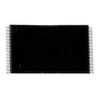
AM29F010B-70EF Spansion Inc., AM29F010B-70EF Datasheet - Page 4

AM29F010B-70EF
Manufacturer Part Number
AM29F010B-70EF
Description
IC, FLASH, 1MBIT, 70NS, TSOP-32
Manufacturer
Spansion Inc.
Specifications of AM29F010B-70EF
Memory Type
Flash
Memory Size
1Mbit
Memory Configuration
128K X 8
Access Time
70ns
Supply Voltage Range
4.5V To 5.5V
Memory Case Style
TSOP
No. Of Pins
32
Cell Type
NOR
Density
1Mb
Access Time (max)
70ns
Interface Type
Parallel
Boot Type
Not Required
Address Bus
17b
Operating Supply Voltage (typ)
5V
Operating Temp Range
-40C to 85C
Package Type
TSOP
Program/erase Volt (typ)
4.5 to 5.5V
Sync/async
Asynchronous
Operating Temperature Classification
Industrial
Operating Supply Voltage (min)
4.5V
Operating Supply Voltage (max)
5.5V
Word Size
8b
Number Of Words
128K
Supply Current
30mA
Mounting
Surface Mount
Pin Count
32
Lead Free Status / RoHS Status
Lead free / RoHS Compliant
Available stocks
Company
Part Number
Manufacturer
Quantity
Price
Part Number:
AM29F010B-70EF
Manufacturer:
AMD
Quantity:
20 000
GENERAL DESCRIPTION
The Am29F010B is a 1 Mbit, 5.0 Volt-only Flash
memory organized as 131,072 bytes. The Am29F010B
is offered in 32-pin PLCC and TSOP packages. The
byte-wide data appears on DQ0-DQ7. The device is
designed to be programmed in-system with the standard
system 5.0 Volt V
for program or erase operations. The device can also be
programmed or erased in standard EPROM programmers.
This device is manufactured using AMD’s 0.32 µm pro-
cess technology, and offers all the features and benefits
of the Am29F010 and Am29F010A.
The standard device offers access times of 45, 55 and
70 ns, allowing high-speed microprocessors to operate
without wait states. To eliminate bus contention the de-
vice has separate chip enable (CE#), write enable
(WE#) and output enable (OE#) controls.
The device requires only a single 5.0 volt power sup-
ply for both read and write functions. Internally
generated and regulated voltages are provided for the
program and erase operations.
The device is entirely command set compatible with the
JEDEC single-power-supply Flash standard. Com-
mands are written to the command register using
standard microprocessor write timings. Register con-
tents serve as input to an internal state machine that
controls the erase and programming circuitry. Write
cycles also internally latch addresses and data needed
for the programming and erase operations. Reading
data out of the device is similar to reading from other
Flash or EPROM devices.
Device programming occurs by executing the program
command sequence. This invokes the Embedded Pro-
g r a m a l g o r i t h m — a n i n t e r n a l a l g o r i t h m t h a t
2
CC
supply. A 12.0 volt V
PP
is not required
D A T A
S H E E T
automatically times the program pulse widths and
verifies proper cell margin.
Device erasure occurs by executing the erase com-
mand sequence. This invokes the Embedded Erase
algorithm—an internal algorithm that automatically
preprograms the array (if it is not already programmed)
before executing the erase operation. During erase, the
device automatically times the erase pulse widths and
verifies proper cell margin.
The host system can detect whether a program or
erase operation is complete by reading the DQ7 (Data#
Polling) and DQ6 (toggle) status bits. After a program
or erase cycle has been completed, the device is ready
to read array data or accept another command.
The sector erase architecture allows memory sectors
to be erased and reprogrammed without affecting the
data contents of other sectors. The device is erased
when shipped from the factory.
The hardware data protection measures include a
low V
during power transitions. The hardware sector protec-
tion feature disables both program and erase operations
in any combination of the sectors of memory, and is im-
plemented using standard EPROM programmers.
The system can place the device into the standby mode.
Power consumption is greatly reduced in this mode.
AMD’s Flash technology combines years of Flash
memory manufacturing experience to produce the
h i g h e s t l eve l s o f q u a l i t y, r e l i a b i l i t y, a n d c o s t
effectiveness. The device electrically erases all bits
within a sector simultaneously via Fowler-Nordheim
tunneling. The bytes are programmed one byte at a
time using the EPROM programming mechanism of hot
electron injection.
CC
detector automatically inhibits write operations
Am29F010B_00_C10 November 12, 2009


