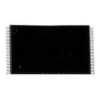
AM29F010B-70EF Spansion Inc., AM29F010B-70EF Datasheet - Page 16

AM29F010B-70EF
Manufacturer Part Number
AM29F010B-70EF
Description
IC, FLASH, 1MBIT, 70NS, TSOP-32
Manufacturer
Spansion Inc.
Specifications of AM29F010B-70EF
Memory Type
Flash
Memory Size
1Mbit
Memory Configuration
128K X 8
Access Time
70ns
Supply Voltage Range
4.5V To 5.5V
Memory Case Style
TSOP
No. Of Pins
32
Cell Type
NOR
Density
1Mb
Access Time (max)
70ns
Interface Type
Parallel
Boot Type
Not Required
Address Bus
17b
Operating Supply Voltage (typ)
5V
Operating Temp Range
-40C to 85C
Package Type
TSOP
Program/erase Volt (typ)
4.5 to 5.5V
Sync/async
Asynchronous
Operating Temperature Classification
Industrial
Operating Supply Voltage (min)
4.5V
Operating Supply Voltage (max)
5.5V
Word Size
8b
Number Of Words
128K
Supply Current
30mA
Mounting
Surface Mount
Pin Count
32
Lead Free Status / RoHS Status
Lead free / RoHS Compliant
Available stocks
Company
Part Number
Manufacturer
Quantity
Price
Part Number:
AM29F010B-70EF
Manufacturer:
AMD
Quantity:
20 000
WRITE OPERATION STATUS
The device provides several bits to determine the sta-
tus of a write operation: DQ3, DQ5, DQ6, and DQ7.
Table 5 and the following subsections describe the
functions of these bits. DQ7 and DQ6 each offer a
method for determining whether a program or erase
operation is complete or in progress. These three bits
are discussed first.
DQ7: Data# Polling
The Data# Polling bit, DQ7, indicates to the host sys-
tem whether an Embedded Algorithm is in progress or
completed. Data# Polling is valid after the rising edge
of the final WE# pulse in the program or erase com-
mand sequence.
During the Embedded Program algorithm, the device
outputs on DQ7 the complement of the datum pro-
grammed to DQ7. When the Embedded Program
algorithm is complete, the device outputs the datum
programmed to DQ7. The system must provide the pro-
gram address to read valid status information on DQ7.
If a program address falls within a protected sector,
Data# Polling on DQ7 is active for approximately 2 µs,
then the device returns to reading array data.
During the Embedded Erase algorithm, Data# Polling
produces a “0” on DQ7. When the Embedded Erase al-
gorithm is complete, Data# Polling produces a “1” on
DQ7. This is analogous to the complement/true datum
output described for the Embedded Program algorithm:
the erase function changes all the bits in a sector to “1”;
prior to this, the device outputs the “complement,” or
“0.” The system must provide an address within any of
the sectors selected for erasure to read valid status in-
formation on DQ7.
After an erase command sequence is written, if all sec-
tors selected for erasing are protected, Data# Polling
on DQ7 is active for approximately 100 µs, then the de-
vice returns to reading array data. If not all selected
sectors are protected, the Embedded Erase algorithm
erases the unprotected sectors, and ignores the se-
lected sectors that are protected.
When the system detects DQ7 has changed from the
complement to true data, it can read valid data at DQ7–
DQ0 on the following read cycles. This is because DQ7
may change asynchronously with DQ0–DQ6 while
Output Enable (OE#) is asserted low. The Data# Poll-
ing Timings (During Embedded Algorithms) figure in
the “AC Characteristics” section illustrates this.
Table 5 shows the outputs for Data# Polling on DQ7.
Figure 3 shows the Data# Polling algorithm.
mand sequence (prior to the program or erase
14
D A T A
S H E E T
DQ6: Toggle Bit I
Toggle Bit I on DQ6 indicates whether an Embedded
Program or Erase algorithm is in progress or complete.
Toggle Bit I may be read at any address, and is valid
after the rising edge of the final WE# pulse in the com-
operation), and during the sector erase time-out.
Notes:
1. VA = Valid address for programming. During a sector
2. DQ7 should be rechecked even if DQ5 = “1” because
No
erase operation, a valid address is an address within any
sector selected for erasure. During chip erase, a valid
address is any non-protected sector address.
DQ7 may change simultaneously with DQ5.
Figure 3. Data# Polling Algorithm
Read DQ7–DQ0
Read DQ7–DQ0
DQ7 = Data?
DQ7 = Data?
Addr = VA
Addr = VA
DQ5 = 1?
START
FAIL
Am29F010B_00_C10 November 12, 2009
No
Yes
No
Yes
Yes
PASS


