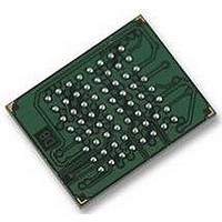
S29GL128P10FFI010 Spansion Inc., S29GL128P10FFI010 Datasheet - Page 63

S29GL128P10FFI010
Manufacturer Part Number
S29GL128P10FFI010
Description
IC, FLASH, 128MBIT, 100NS, BGA-64
Manufacturer
Spansion Inc.
Datasheet
1.S29GL128P10FFI010.pdf
(80 pages)
Specifications of S29GL128P10FFI010
Memory Type
Flash
Memory Size
128Mbit
Memory Configuration
16M X 8 / 8M X 16
Ic Interface Type
CFI, Parallel
Access Time
100ns
Supply Voltage Range
2.7 To 3.6 V
Memory Case Style
BGA
Cell Type
NOR
Density
128Mb
Access Time (max)
100ns
Interface Type
Parallel
Boot Type
Not Required
Address Bus
24/23Bit
Operating Supply Voltage (typ)
3/3.3V
Operating Temp Range
-40C to 85C
Package Type
Fortified BGA
Sync/async
Asynchronous
Operating Temperature Classification
Industrial
Operating Supply Voltage (min)
2.7V
Operating Supply Voltage (max)
3.6V
Word Size
8/16Bit
Number Of Words
16M/8M
Supply Current
110mA
Mounting
Surface Mount
Pin Count
64
Rohs Compliant
Yes
Lead Free Status / RoHS Status
Lead free / RoHS Compliant
Available stocks
Company
Part Number
Manufacturer
Quantity
Price
Company:
Part Number:
S29GL128P10FFI010
Manufacturer:
XILINX
Quantity:
364
Part Number:
S29GL128P10FFI010
Manufacturer:
SPANSION
Quantity:
20 000
Company:
Part Number:
S29GL128P10FFI010A
Manufacturer:
SPANSION
Quantity:
10 393
Notes
1. SA = sector address (for Sector Erase), VA = Valid Address for reading status data (see
2. These waveforms are for the word mode
Notes
1. VA = Valid address. Illustration shows first status cycle after command sequence, last status read cycle, and array data read cycle.
2. t
3. CE# does not need to go high between status bit reads
November 17, 2010 S29GL-P_00_A13
Addresses
OE
Addresses
DQ6–DQ0
RY/BY#
for data polling is 45 ns when V
RY/BY#
WE#
DQ7
OE#
CE#
WE#
Data
CE#
OE#
V
CC
t
VCS
t
t
BUSY
CH
t
OEH
t
Erase Command Sequence (last two cycles)
CS
2AAh
Figure 11.12 Data# Polling Timings (During Embedded Algorithms)
t
IO
WC
t
= 1.65 to 2.7 V and is 35 ns when V
ACC
t
CE
t
t
VA
t
WP
t
RC
OE
DS
Figure 11.11 Chip/Sector Erase Operation Timings
55h
t
t
DH
CH
Complement
Status Data
D a t a
555h for chip erase
t
S29GL-P MirrorBit
WPH
t
OH
t
DF
t
AS
S h e e t
SA
10 for Chip Erase
IO
= 2.7 to 3.6 V
t
AH
®
VA
30h
Complement
Flash Family
Status Data
Write Operation Status on page
t
BUSY
True
True
t
WHWH2
Read Status Data
VA
36.)
Progress
VA
In
Valid Data
Valid Data
VA
Complete
t
RB
High Z
High Z
63


