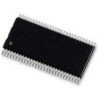
DS90C383BMT National Semiconductor, DS90C383BMT Datasheet

DS90C383BMT
Specifications of DS90C383BMT
Available stocks
Related parts for DS90C383BMT
DS90C383BMT Summary of contents
Page 1
... LVDS devices for low EMI n PLL requires no external components n Compatible with TIA/EIA-644 LVDS standard n Low profile 56-lead TSSOP package n Improved replacement for: SN75LVDS83, DS90C383A DS90C383B Order Number DS90C383BMT See NS Package Number MTD56 DS200984 October 2006 ± 2.5% center < ...
Page 2
... Absolute Maximum Ratings If Military/Aerospace specified devices are required, please contact the National Semiconductor Sales Office/ Distributors for availability and specifications. Supply Voltage ( CMOS/TTL Input Voltage LVDS Driver Output Voltage LVDS Output Short Circuit Duration Junction Temperature Storage Temperature Lead Temperature (Soldering, 4 sec) ...
Page 3
Electrical Characteristics Over recommended operating supply and temperature ranges unless otherwise specified. Symbol Parameter TRANSMITTER SUPPLY CURRENT ICCTG Transmitter Supply Current 16 Grayscale ICCTZ Transmitter Supply Current Power Down Note 1: “Absolute Maximum Ratings” are those values beyond which the ...
Page 4
Transmitter Switching Characteristics Over recommended operating supply and temperature ranges unless otherwise specified Symbol TPPos0 Transmitter Output Pulse Position for Bit 0 (Figure 11 ) (Note 5) TPPos1 Transmitter Output Pulse Position for Bit 1 TPPos2 Transmitter Output Pulse Position ...
Page 5
AC Timing Diagrams FIGURE 2. “16 Grayscale” Test Pattern (Notes 10) Note 7: The worst case test pattern produces a maximum toggling of digital circuits, LVDS I/O and CMOS/TTL I/O. Note 8: The 16 grayscale test pattern ...
Page 6
AC Timing Diagrams FIGURE 3. DS90C383B (Transmitter) LVDS Output Load FIGURE 4. DS90C383B (Transmitter) LVDS Transition Times FIGURE 5. DS90C383B (Transmitter) Input Clock Transition Time FIGURE 6. DS90C383B (Transmitter) Setup/Hold and High/Low Times (Falling Edge Strobe) FIGURE 7. DS90C383B (Transmitter) ...
Page 7
AC Timing Diagrams (Continued) FIGURE 8. DS90C383B (Transmitter) Phase Lock Loop Set Time FIGURE 9. 28 Parallel TTL Data Inputs Mapped to LVDS Outputs FIGURE 10. Transmitter Power Down Delay 7 20098414 20098417 20098418 www.national.com ...
Page 8
AC Timing Diagrams FIGURE 11. Transmitter LVDS Output Pulse Position Measurement DS90C383B Pin Description—FPD Link Transmitter Pin Name I/O No. TxIN I 28 TTL level input. This includes: 8 Red, 8 Green, 8 Blue, and 4 control lines — FPLINE, ...
Page 9
Applications Information The DS90C383B are backward compatible with the DS90C383/DS90CF383, DS90C383A/DS90CF383A and are a pin-for-pin replacement. This device may also be used as a replacement for the DS90CF583 (5V, 65MHz) and DS90CF581 (5V, 40MHz) FPD-Link Transmitters with certain modifications: 1. ...
Page 10
Pin Diagram www.national.com DS90C383B Typical Application TABLE 1. Programmable Transmitter (DS90C383B) Pin Condition Strobe Status R_FB R_FB = V Rising edge strobe CC R_FB R_FB = GND or NC Falling edge strobe 10 20098423 20098403 ...
Page 11
... Tel: 1-800-272-9959 Deutsch Tel: +49 (0) 69 9508 6208 English www.national.com Français Tel: +33 ( 8790 Order Number DS90C383BMT NS Package Number MTD56 2. A critical component is any component of a life support device or system whose failure to perform can be reasonably expected to cause the failure of the life support device or system affect its safety or effectiveness ...


