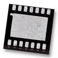
LP3947ISD-51 National Semiconductor, LP3947ISD-51 Datasheet - Page 5

LP3947ISD-51
Manufacturer Part Number
LP3947ISD-51
Description
CHARGER, USB, I2C, POWERWISE, LLP-14
Manufacturer
National Semiconductor
Datasheet
1.LP3947ISD-51.pdf
(14 pages)
Specifications of LP3947ISD-51
Battery Type
Li-Ion
Input Voltage
6V
Battery Charge Voltage
4.2V
Charge Current Max
750mA
Battery Ic Case Style
LLP
No. Of Pins
14
No. Of Series Cells
1
Operating Temperature Range
-40°C
Lead Free Status / RoHS Status
Lead free / RoHS Compliant
Available stocks
Company
Part Number
Manufacturer
Quantity
Price
Company:
Part Number:
LP3947ISD-51/NOPB
Manufacturer:
SONY
Quantity:
6 242
BATTERY CHARGER
V
R
ICHG
t
V
TEMPERATURE SENSE COMPARATORS
V
V
V
V
LDO MODE (Ts = HIGH)
V
LOGIC LEVELS
V
V
I
I
V
V
V
V
F
t
t
t
OUT
IL
IH
HOLD
CLK-LP
CLK-HP
Symbol
CLK
Electrical Characteristics
BAT-RST
OL
UTLO
OTLO
LDO
T
OUT
IL
IH
IL
IH
OL
HYS
SENSE
Unless otherwise noted, V
mal type apply for T
T
Electrical Characteristics, I
Unless otherwise noted, V
25˚C. Limits appearing in boldface type apply over the entire junction temperature range for operation, T
(Notes 7, 8, 9)
Symbol
J
= −40˚C to +85˚C. (Notes 7, 8, 9)
MON
Low Level Input Voltage
High Level Input Voltage
Low Level Output Voltage
Schmitt Trigger Input Hysteresis
Clock Frequency
Hold Time Repeated START
Condition
CLK Low Period
CLK High Period
Restart Threshold Voltage
(For 4.1V Cell)
Restart Threshold Voltage
(For 4.2V Cell)
Internal Current Sense Resistance
Internal Current Sense Resistor
Load Current
Diff-Amp Output
Charger Time Out
Low Level Output Voltage
Low Voltage Threshold
High Voltage Threshold
LDO Mode Voltage Threshold
Voltage Output
Output Voltage Regulation
Low Level Input Voltage
High Level Input Voltage
Input Current
Input Current
J
= 25˚C. Limits appearing in boldface type apply over the entire junction temperature range for operation,
Parameter
Parameter
CHG-IN
CHG-IN
= 5V, V
= V
DD
= 5V, V
BATT
(Continued)
2
= 4V, C
C Interface
BATT
SDA & SCL (Note 8)
SDA & SCL (Note 8)
SDA & SCL (Note 8)
SDA & SCL (Note 8)
(Note 8)
(Note 8)
(Note 8)
(Note 8)
V
to Pre-Qualification State
V
to Pre-Qualification State
(Note 8)
I
I
I
T
T
EOC, CHG Pins each at 9 mA
Voltage at Ts Pin, Rising
Voltage at Ts Pin, Falling
Voltage at Ts Pin, Rising
Voltage at Ts Pin, Falling
Voltage at Ts Pin, % of V
I
I
EN, ISEL, MODE
EN, ISEL, MODE
EN, ISEL = LOW
MODE = LOW
EN, ISEL, MODE = HIGH
CHG
CHG
CHG
LOAD
LOAD
BATT
BATT
J
J
= 4V. Typical values and limits appearing in normal type apply for T
CHG-IN
= 0˚C to 85˚C
= −40˚C to +85˚C
= 50 mA
= 100 mA
= 750 mA
= 50 mA
= 750 mA
Falling, Transition from EOC,
Falling, Transition from EOC,
= 1 µF, C
Conditions
5
Conditions
BATT
= 10 µF. Typical values and limits appearing in nor-
T
Typ
0.583
0.663
1.790
5.625
5.625
2.427
2.369
1.470
1.390
2.787
4.00
4.10
4.06
Typ
120
100
3.9
97
0.7 V
0.1 V
Min
0.4
0.6
1.3
0.6
3.77
3.86
4.78
Min
−10
0
4.5
2.0
−5
−5
DD
DD
J
Limit
Limit
= −40˚C to +125˚C.
V
0.3 V
0.2 V
DD
Max
Max
4.02
4.12
6.42
6.75
400
+10
1.2
0.4
+5
+5
+0.5
www.national.com
DD
DD
J
Units
Units
=
kHz
mΩ
Hrs
mV
µA
µA
µA
µs
µs
µs
%
V
A
V
V
V
V
V
V
V
V
V
V
V


