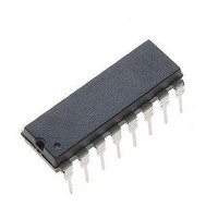
DG309BDJ-E3 Vishay, DG309BDJ-E3 Datasheet

DG309BDJ-E3
Specifications of DG309BDJ-E3
Related parts for DG309BDJ-E3
DG309BDJ-E3 Summary of contents
Page 1
... DESCRIPTION The DG308B, DG309B analog switches are highly improved versions of the industry-standard DG308A, DG309. These devices are fabricated in Vishay Siliconix’ proprietary silicon gate CMOS process, resulting in lower on-resistance, lower leakage, higher speed, and lower power consumption. These quad single-pole single-throw switches are designed for a wide variety of applications in telecommunications, instrumentation, process control, computer peripherals, etc ...
Page 2
... Derate 7.6 mW/°C above 75 °C. e. Derate 12 mW/°C above 75 °C. www.vishay.com 2 Package 16-Pin PlasticDIP 16-Pin Narrow SOIC 16-Pin TSSOP 30 mA, whichever occurs first Part Number DG308BDJ DG308BDJ-E3 DG309BDJ DG309BDJ-E3 DG308BDY DG308BDY-E3 DG308BDY-T1 DG308BDY-T1-E3 DG309BDY DG309BDY-E3 DG309BDY-T1 DG309BDY-T1-E3 DG308BDQ DG308BDQ-E3 DG308BDQ-T1 DG308BDQ-T1-E3 DG309BDQ DG309BDQ-E3 DG309BDQ-T1 ...
Page 3
... MHz, S Room MHz Room D S Room = 50 pF 100 kHz Room S RMS Room Full Room Full Full DG308B, DG309B Vishay Siliconix A Suffix D Suffix - 55 °C to 125 ° ° ° Typ. Min. Max. Min. Max 100 100 2 ± 0.01 - 0.5 0 ± ...
Page 4
... DG308B, DG309B Vishay Siliconix a SPECIFICATIONS (for Single Supply) Parameter Symbol Analog Switch e Analog Signal Range V ANALOG Drain-Source R DS(on) On-Resistance Dynamic Characteristics Turn-On Time t ON Turn-Off Time t OFF Charge Injection Q Power Supply Positive Supply Current I+ Negative Supply Current I- Power Supply Range for ...
Page 5
... ± 100 D( Temperature (°C) Leakage Currents vs. Temperature Document Number: 70047 S11-0303-Rev. G, 28-Feb-11 100 ± ± ± 105 125 DG308B, DG309B Vishay Siliconix 125 ° ° ° ° Drain Voltage ( vs. V and Temperature DS(on ° D(on Analog Voltage Leakage Currents vs. Analog Voltage ...
Page 6
... DG308B, DG309B Vishay Siliconix TYPICAL CHARACTERISTICS (25 °C, unless otherwise noted) SCHEMATIC DIAGRAM (Typical Channel GND V– www.vishay.com 6 120 100 100 Frequency (Hz) Off Isolation vs. Frequency Level Shift/ Drive Figure Document Number: 70047 S11-0303-Rev. G, 28-Feb-11 ...
Page 7
... GND - 15 V Document Number: 70047 S11-0303-Rev. G, 28-Feb-11 Logic Input k Switch Output DS(on) Figure 2. Switching Time bypass X Isolation = 20 log 1000 pF V- Figure 5. Charge Injection DG308B, DG309B Vishay Siliconix t < < OFF GND Figure 4. Channel-to-Channel Crosstalk OFF IN X V = measured voltage error due to charge injection O x ...
Page 8
... DG308B, DG309B Vishay Siliconix APPLICATIONS + IN1 V IN2 DG419 CH GND Gain Gain = Gain Gain 3 (x 100) Gain 4 (x 1000) Logic High = Switch On Figure 6. A Precision Amplifier with Digitally Programmable Inputs and Gains + LM101A M IN 5.1 M Aquisition T ime = 25 µs Aperature T ime = 1 µ ...
Page 9
... Figure 8. Active Low Pass Filter with Digitally Selected Break Frequency Vishay Siliconix maintains worldwide manufacturing capability. Products may be manufactured at one of several qualified locations. Reliability data for Silicon Technology and Package Reliability represent a composite of all qualified locations. For related documents such as package/tape drawings, part marking, and reliability data, see www ...
Page 10
... Vishay product could result in personal injury or death. Customers using or selling Vishay products not expressly indicated for use in such applications their own risk and agree to fully indemnify and hold Vishay and its distributors harmless from and against any and all claims, liabilities, expenses and damages arising or resulting in connection with such use or sale, including attorneys fees, even if such claim alleges that Vishay or its distributor was negligent regarding the design or manufacture of the part ...


