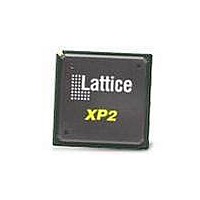
LFXP2-5E-5FTN256C Lattice, LFXP2-5E-5FTN256C Datasheet - Page 75

LFXP2-5E-5FTN256C
Manufacturer Part Number
LFXP2-5E-5FTN256C
Description
FPGA - Field Programmable Gate Array 5K LUTs 172I/O Inst- on DSP 1.2V -5 Spd
Manufacturer
Lattice
Series
LatticeXP2r
Datasheet
1.LFXP2-40E-5FN484I.pdf
(92 pages)
Specifications of LFXP2-5E-5FTN256C
Number Of Macrocells
5000
Maximum Operating Frequency
200 MHz
Number Of Programmable I/os
172
Data Ram Size
10 KB
Supply Voltage (max)
1.14 V
Supply Current
17 mA
Maximum Operating Temperature
+ 85 C
Minimum Operating Temperature
0 C
Mounting Style
SMD/SMT
Supply Voltage (min)
1.26 V
Package / Case
FTBGA-256
No. Of Logic Blocks
5000
No. Of Macrocells
2500
Family Type
LatticeXP2
No. Of Speed Grades
5
Total Ram Bits
166Kbit
No. Of I/o's
172
Clock Management
PLL
Rohs Compliant
Yes
Lead Free Status / RoHS Status
Lead free / RoHS Compliant
Available stocks
Company
Part Number
Manufacturer
Quantity
Price
Company:
Part Number:
LFXP2-5E-5FTN256C
Manufacturer:
LATTICE
Quantity:
1 001
Company:
Part Number:
LFXP2-5E-5FTN256C
Manufacturer:
Lattice Semiconductor Corporation
Quantity:
10 000
Part Number:
LFXP2-5E-5FTN256C
Manufacturer:
LATTICE
Quantity:
20 000
Lattice Semiconductor
FlashBAK Time (from EBR to Flash)
JTAG Port Timing Specifications
XP2-5
XP2-8
XP2-17
XP2-30
XP2-40
f
t
t
t
t
t
t
t
t
t
t
t
t
t
t
Timing v. A 0.12
MAX
BTCP
BTCPH
BTCPL
BTS
BTH
BTRF
BTCO
BTCODIS
BTCOEN
BTCRS
BTCRH
BUTCO
BTUODIS
BTUPOEN
Symbol
Device
TCK Clock Frequency
TCK [BSCAN] clock pulse width
TCK [BSCAN] clock pulse width high
TCK [BSCAN] clock pulse width low
TCK [BSCAN] setup time
TCK [BSCAN] hold time
TCK [BSCAN] rise/fall time
TAP controller falling edge of clock to valid output
TAP controller falling edge of clock to valid disable
TAP controller falling edge of clock to valid enable
BSCAN test capture register setup time
BSCAN test capture register hold time
BSCAN test update register, falling edge of clock to valid output
BSCAN test update register, falling edge of clock to valid disable
BSCAN test update register, falling edge of clock to valid enable
EBR Density (Bits)
Over Recommended Operating Conditions
Over Recommended Operating Conditions
166K
221K
276K
387K
885K
Parameter
3-31
Time (Typ.)
1.5
1.5
1.5
2.0
3.0
DC and Switching Characteristics
LatticeXP2 Family Data Sheet
Min.
25
—
40
20
20
10
50
—
—
—
—
—
—
8
8
Max.
10
10
10
25
25
25
25
—
—
—
—
—
—
—
—
Units
s
s
s
s
s
mV/ns
Units
MHz
ns
ns
ns
ns
ns
ns
ns
ns
ns
ns
ns
ns
ns


