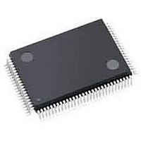
APA075-TQG100 Actel, APA075-TQG100 Datasheet - Page 78

APA075-TQG100
Manufacturer Part Number
APA075-TQG100
Description
FPGA - Field Programmable Gate Array 75K System Gates
Manufacturer
Actel
Datasheet
1.APA075-FGG144.pdf
(178 pages)
Specifications of APA075-TQG100
Processor Series
APA075
Core
IP Core
Maximum Operating Frequency
150 MHz
Number Of Programmable I/os
158
Data Ram Size
27648
Supply Voltage (max)
2.7 V
Maximum Operating Temperature
+ 70 C
Minimum Operating Temperature
0 C
Development Tools By Supplier
APA-Eval-Kit, APA-Eval-BRD1, Silicon-Explorer II, Silicon-Sculptor 3, SI-EX-TCA, Flashpro 4, Flashpro 3, Flashpro Lite
Mounting Style
SMD/SMT
Supply Voltage (min)
2.3 V
Number Of Gates
75 K
Package / Case
TQFP-100
Lead Free Status / RoHS Status
Lead free / RoHS Compliant
Available stocks
Company
Part Number
Manufacturer
Quantity
Price
Part Number:
APA075-TQG100
Manufacturer:
ACTEL
Quantity:
20 000
Company:
Part Number:
APA075-TQG100A
Manufacturer:
Microsemi SoC
Quantity:
10 000
Company:
Part Number:
APA075-TQG100I
Manufacturer:
Microsemi SoC
Quantity:
10 000
Part Number:
APA075-TQG100I
Manufacturer:
ACTEL/爱特
Quantity:
20 000
Asynchronous FIFO Write
Note: The plot shows the normal operation status.
Figure 2-41 • Asynchronous FIFO Write
Table 2-64 • T
2 -6 8
Symbol t
DWRH
DWRS
DWRS
EWRH, FWRH,
THWRH
EWRA
FWRA
THWRA
WPDA
WPDH
WRCYC
WRRDS
WRH
WRL
Notes:
1. At fast cycles, EWRA, FWRA = MAX (7.5 ns – WRL), 3.0 ns.
2. At fast cycles, WRRDS (for enabling write) = MAX (7.5 ns – RDL), 3.0 ns.
3. After FIFO reset, WRB needs an initial falling edge prior to any write actions.
ProASIC
PLUS
xxx
T
J
J
Flash Family FPGAs
= 0°C to 110°C; V
= –55°C to 150°C, V
DI setup to WB ↑
DI setup to WB ↑
Old EMPTY, FULL, EQTH, & GETH valid hold
time after WB ↑
WB ↓
DI hold from WB ↑
EMPTY ↓ access from WB ↑
New FULL access from WB ↑
EQTH or GETH access from WB ↑
WPE access from DI
WPE hold from DI
Cycle time
RB ↑, clearing FULL, setup to
WB high phase
WB low phase
WB = (WRB + WBLKB)
Description
DD
DD
= 2.3 V to 2.7 V for Commercial/Industrial
EQTH, GETH
= 2.3 V to 2.7 V for Military/MIL-STD-883
WDATA
EMPTY
t WRRDS
FULL
WPE
RB
t WPDA
t EWRH , t FWRH
t EWRA , t FWRA
t DWRS
Cycle Start
t WRL
Min.
3.0
3.0
3.0
1.5
0.5
2.5
4.5
3.0
7.5
3.0
3.0
v5.9
1
1
2
t WRCYC
Max.
0.5
1.0
1.0
t THWRH
t THWRA
t WRH
Units
ns
ns
ns
ns
ns
ns
ns
ns
ns
ns
ns
ns
ns
(Full inhibits write)
t DWRH
t WPDH
PARGEN is inactive
PARGEN is active
Empty/full/thresh are invalid from the end
of hold until the new access is complete
WPE is invalid while PARGEN is active
Enabling the write operation
Inhibiting the write operation
Inactive
Active
Notes


