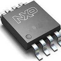
PCA9507DP,118 NXP Semiconductors, PCA9507DP,118 Datasheet - Page 12

PCA9507DP,118
Manufacturer Part Number
PCA9507DP,118
Description
I/O Expanders, Repeaters & Hubs LEVEL TRANSL I2C BUS
Manufacturer
NXP Semiconductors
Series
-r
Datasheet
1.PCA9507DP118.pdf
(20 pages)
Specifications of PCA9507DP,118
Logic Family
SDA, SCL
Propagation Delay Time
218 ns
Operating Supply Voltage
2.7 V to 5.5 V
Power Dissipation
100 mW
Operating Temperature Range
- 40 C to + 85 C
Logic Type
I2C Bus
Mounting Style
SMD/SMT
Output Current
50 mA
Output Voltage
0.52 V
Package / Case
TSSOP-8
Mounting Type
Surface Mount
Voltage - Supply
2.7 V ~ 5.5 V
Operating Temperature
-40°C ~ 85°C
Interface
I²C, SMBus
Number Of I /o
24
Frequency - Clock
400kHz
Interrupt Output
No
Includes
-
Lead Free Status / RoHS Status
Lead free / RoHS Compliant
Lead Free Status / RoHS Status
Lead free / RoHS Compliant, Lead free / RoHS Compliant
Other names
935285824118 PCA9507DP-T
Available stocks
Company
Part Number
Manufacturer
Quantity
Price
Company:
Part Number:
PCA9507DP,118
Manufacturer:
MCC
Quantity:
40 000
Part Number:
PCA9507DP,118
Manufacturer:
NXP/恩智浦
Quantity:
20 000
NXP Semiconductors
Table 5.
V
[1]
[2]
[3]
10. Dynamic characteristics
Table 6.
V
[1]
[2]
[3]
[4]
[5]
[6]
PCA9507_1
Product data sheet
Symbol
Enable
V
V
I
I
C
Symbol
t
t
t
t
t
t
t
t
t
t
IL(EN)
LI
PLH
PHL
TLH
THL
PLH
PHL
TLH
THL
su
h
CC
CC
IL
IH
i
= 2.7 V to 5.5 V; GND = 0 V; T
LOW-level supply voltage.
V
SDAB/SCLB lines.
V
= 2.7 V to 5.5 V; GND = 0 V; T
Times are specified with loads of 1.35 k pull-up resistance and 57 pF load capacitance on port B, and 450
57 pF load capacitance on port A. Different load resistance and capacitance will alter the RC time constant, thereby changing the
propagation delay and transition times.
Pull-up voltages are V
Typical values were measured with V
The t
The proportional delay data from port A to port B is measured at 0.3V
The enable pin, EN, should only change state when the global bus and the repeater port are in an idle state.
IL
IL
specification is for the first LOW level seen by the SDAB/SCLB lines. V
for port A with envelope noise must be below 0.3V
PLH
Parameter
LOW-to-HIGH propagation delay
HIGH-to-LOW propagation delay
LOW to HIGH output transition time port A;
HIGH to LOW output transition time port A;
LOW-to-HIGH propagation delay
HIGH-to-LOW propagation delay
LOW to HIGH output transition time port B;
HIGH to LOW output transition time port B;
set-up time
hold time
Static characteristics
Dynamic characteristics
delay data from port B to port A is measured at 0.5 V on port B to 0.3V
Parameter
LOW-level input voltage
HIGH-level input voltage
LOW-level input current on pin
EN
input leakage current
input capacitance
CC(A)
on port A and V
amb
amb
…continued
CC(A)
= 40 C to +85 C; unless otherwise specified.
= 40 C to +85 C; unless otherwise specified.
= 3.3 V at T
CC(B)
on port B.
Conditions
V
V
V
Conditions
port B to port A;
port B to port A;
port A to port B;
port A to port B;
EN HIGH before START condition
EN HIGH after STOP condition
Rev. 01 — 7 February 2008
I
I
I
= 0.2 V, EN; V
= V
= 3.0 V or 0 V
CC(A)
2-wire serial bus extender for HDMI DDC I
amb
CC
= 25 C, unless otherwise noted.
Figure 13
Figure 13
Figure 14
Figure 14
for stable performance.
CC
Figure 15
Figure 13
Figure 14
Figure 14
CC(A)
= 3.6 V
ILc
on port A to 0.3V
is for the second and subsequent LOW levels seen by the
CC(A)
on port A.
[1][2]
CC(B)
[4]
[5]
[5]
[6]
[6]
Min
0.7V
-
-
0.5
1
Min
90
55
22
20
140
130
100
20
100
100
on port B.
CC(B)
Typ
-
-
-
6
10
Typ
165
91
48
42
218
91
173
39
-
-
2
PCA9507
pull-up resistance and
C-bus and SMBus
© NXP B.V. 2008. All rights reserved.
[3]
Max
+0.3V
+1
5.5
7
30
Max
350
180
80
100
310
330
260
100
-
-
CC(B)
12 of 20
Unit
ns
ns
ns
ns
ns
ns
ns
ns
ns
ns
Unit
V
V
pF
A
A


