VN2210N3-G Supertex, VN2210N3-G Datasheet

MOSFET Small Signal 100V 0.35Ohm

VN2210N3-G

Manufacturer Part Number
VN2210N3-G
Description
MOSFET Small Signal 100V 0.35Ohm
Manufacturer
Supertex
Datasheet

Specifications of VN2210N3-G

Minimum Operating Temperature
- 55 C
Configuration
Single
Transistor Polarity
N-Channel
Resistance Drain-source Rds (on)
0.35 Ohm @ 10 V
Drain-source Breakdown Voltage
100 V
Gate-source Breakdown Voltage
+/- 20 V
Continuous Drain Current
1.2 A
Power Dissipation
1000 mW
Maximum Operating Temperature
+ 150 C
Mounting Style
Through Hole
Package / Case
TO-92
Lead Free Status / RoHS Status
Lead free / RoHS Compliant
Features
Applications
-G
Absolute Maximum Ratings
Absolute Maximum Ratings are those values beyond which damage to
the device may occur. Functional operation under these conditions is not
implied. Continuous operation of the device at the absolute rating level
may affect device reliability. All voltages are referenced to device ground.
*
Supertex inc.
Ordering Information
Parameter
Drain-to-source voltage
Drain-to-gate voltage
Gate-to-source voltage
Operating and storage temperature
Soldering temperature*
Distance of 1.6mm from case for 10 seconds.
indicates package is RoHS compliant (‘Green’)
package is RoHS compliant (‘Green’)
Free from secondary breakdown
Low power drive requirement
Ease of paralleling
Low C
Excellent thermal stability
Integral source-drain diode
High input impedance and high gain
Motor controls
Converters
Amplifiers
Switches
Power supply circuits
Drivers (relays, hammers, solenoids, lamps,
memories, displays, bipolar transistors, etc.)
VN2210
Device
ISS
Supertex inc.
and fast switching speeds
VN2210N2
TO-39
Package Options
N-Channel Enhancement-Mode
Vertical DMOS FETs
1235 Bordeaux Drive, Sunnyvale, CA 94089
-55°C to +150°C
VN2210N3-G
+300°C
TO-92
Value
BV
BV
±20V
DGS
DSS
General Description
The Supertex VN2210 is an enhancement-mode (normally-
off) transistor that utilizes a vertical DMOS structure
and Supertex’s well-proven silicon-gate manufacturing
process. This combination produces a device with the
power handling capabilities of bipolar transistors, and the
high input impedance and positive temperature coefficient
inherent in MOS devices. Characteristic of all MOS
structures, this device is free from thermal runaway and
thermally-induced secondary breakdown.
Supertex’s vertical DMOS FETs are ideally suited to a
wide range of switching and amplifying applications where
very low threshold voltage, high breakdown voltage, high
input impedance, low input capacitance, and fast switching
speeds are desired.
Pin Configurations
Product Marking
Package may or may not include the following marks: Si or
BV
SOURCE
TO-39 (N2)
DSS
Y Y W W
2 2 1 0
100
Si VN
(V)
Tel: 408-222-8888
/BV
GATE
DGS
DRAIN
YYWW
2210N2
YY = Year Sealed
WW = Week Sealed
VN
TO-92 (N3)
TO-39 (N2)
YY = Year Sealed
WW = Week Sealed
= “Green” Packaging
R
(max)
0.35
www.supertex.com
DS(ON)
(Ω)
SOURCE
TO-92 (N3)
VN2210
DRAIN
GATE
I
(min)
D(ON)
8.0
(A)

Related parts for VN2210N3-G

VN2210N3-G Summary of contents

Page 1

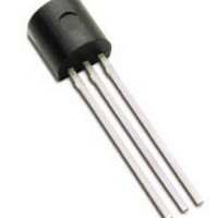
... Supertex’s vertical DMOS FETs are ideally suited to a wide range of switching and amplifying applications where very low threshold voltage, high breakdown voltage, high input impedance, low input capacitance, and fast switching speeds are desired. TO-92 VN2210N3-G † Pin Configurations Product Marking Value BV ...

Page 2

... SD t Reverse recovery time rr Notes: 1. All D.C. parameters 100% tested All A.C. parameters sample tested. Switching Waveforms and Test Circuit 10V INPUT 10 (ON) t d(ON) VDD 10% OUTPUT 0V Supertex inc. ● I Power Dissipation D (pulsed (A) (W) 10 6.0 8.0 1 25°C unless otherwise specified) A ...

Page 3

... Transconductance vs. Drain Current 4 3.2 2.4 1.6 0 0.8 1.6 I (amperes) D Maximum Rated Safe Operating Area 10 TO-92 (pulsed) TO-39 (DC) 1 TO-92 (DC) 0 0.01 0 (volts) DS Supertex inc 10V 150 C O 2.4 3.2 4.0 TO-39 (pulsed) 10 100 ● 1235 Bordeaux Drive, Sunnyvale, CA 94089 3 Saturation Characteristics 10V ...

Page 4

... Transfer Characteristics - (volts) GS Capacitance vs. Drain-to-Source Voltage 500 f = 1.0MHz 375 250 125 (volt) DS Supertex inc. (cont.) 100 150 150 ISS C OSS C RSS 30 40 ● 1235 Bordeaux Drive, Sunnyvale, CA 94089 4 On-Resistance vs. Drain Current 1 5. 10V GS 0.6 0.4 0 (amperes and RV ...

Page 5

... Bottom View Symbol α MIN Dimension 45 O NOM (inches) NOM NOM MAX JEDEC Registration TO-39. * This dimension is not specified in the JEDEC drawing. Drawings not to scale. Supertex Doc. #: DSPD-3TO39N2, Version B052009. Supertex inc. β β A Φa Φb .240 .190 .016 ...

Page 6

... This dimension is not specified in the JEDEC drawing. † This dimension differs from the JEDEC drawing. Drawings not to scale. Supertex Doc.#: DSPD-3TO92N3, Version E041009. (The package drawing(s) in this data sheet may not reflect the most current specifications. For the latest package outline information go to http://www.supertex.com/packaging.html.) does not recommend the use of its products in life support applications, and will not knowingly sell them for use in such applications unless it receives Supertex inc ...

Related keywords