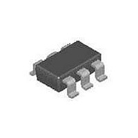
FDC658AP Fairchild Semiconductor, FDC658AP Datasheet - Page 4

FDC658AP
Manufacturer Part Number
FDC658AP
Description
MOSFET Small Signal -30VSgl P-Chl LogLv PwrTrch MOSFET
Manufacturer
Fairchild Semiconductor
Type
Power MOSFETr
Datasheet
1.FDC658AP.pdf
(5 pages)
Specifications of FDC658AP
Minimum Operating Temperature
- 55 C
Configuration
Single Quad Drain
Transistor Polarity
P-Channel
Resistance Drain-source Rds (on)
0.05 Ohm @ 10 V
Forward Transconductance Gfs (max / Min)
8.4 S
Drain-source Breakdown Voltage
30 V
Gate-source Breakdown Voltage
+/- 25 V
Continuous Drain Current
4 A
Power Dissipation
1600 mW
Maximum Operating Temperature
+ 150 C
Mounting Style
SMD/SMT
Package / Case
SuperSOT
Number Of Elements
1
Polarity
P
Channel Mode
Enhancement
Drain-source On-res
0.05Ohm
Drain-source On-volt
30V
Gate-source Voltage (max)
±25V
Output Power (max)
Not RequiredW
Frequency (max)
Not RequiredMHz
Noise Figure
Not RequireddB
Power Gain
Not RequireddB
Drain Efficiency
Not Required%
Operating Temp Range
-55C to 150C
Operating Temperature Classification
Military
Mounting
Surface Mount
Pin Count
6
Package Type
SuperSOT
Lead Free Status / RoHS Status
Lead free / RoHS Compliant
Available stocks
Company
Part Number
Manufacturer
Quantity
Price
Company:
Part Number:
FDC658AP
Manufacturer:
Fairchild Semiconductor
Quantity:
140 672
Part Number:
FDC658AP
Manufacturer:
FAIRCHILD/仙童
Quantity:
20 000
Part Number:
FDC658AP-NL
Manufacturer:
FAIRCHILD/仙童
Quantity:
20 000
FDC658AP Rev. B (W)
Typical Characteristics
Figure 9.
Figure 7.
0.01
100
0.1
10
10
8
6
4
2
0
1
0.001
0.1
0.01
0
0.1
0.00001
r
I
DS(on)
1
D
SINGLE PULSE
R
= -4A
θJA
V
Forward Bias Safe Operating Area
T
GS
A
LIMIT
= 156
= 25
D = 0.5
= -10V
Gate Charge Characteristics
0.2
0.1
2
0.05
o
o
-V
0.02
C
C/W
0.01
DS
, DRAIN TO SOURCE VOLTAGE (V)
Thermal characterization performed using the conditions described in Note 1b.
Transient thermal response will change depending on the circuit board design.
0.0001
Q
1
SINGLE PULSE
g
, GATE CHARGE (nC)
4
Figure 11.
0.001
6
V
10
DS
= -5V
Transient Thermal Response Curve
8
-15V
t, RECTANGULAR PULSE DURATION
100us
100ms
1ms
10ms
1s
DC
0.01
-10V
100
10
4
Figure 8.
0.1
Figure 10.
600
450
300
150
10
8
6
4
2
0
0
0.01
0
Capacitance vs Drain to Source Voltage
C
1
rss
6
Single Pulse Maximum Power
-V
C
0.1
oss
DS
, DRAIN TO SOURCE VOLTAGE (V)
Dissipation
t, PULSE WIDTH (s)
10
12
C
iss
1
P(pk)
Duty Cycle, D = t
T
R
J
R
θJA
- T
θJA
18
(t) = r(t) + R
A
= 156
t
100
1
= P * R
t
2
www.fairchildsemi.com
o
SINGLE PULSE
C/W
R
10
θJA
θJA
T
1
θJA
24
A
(t)
/ t
= 156°C/W
= 25°C
2
f = 1 MHz
V
GS
1000
= 0 V
100
30


