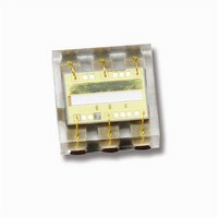
TSL2561T TAOS, TSL2561T Datasheet - Page 15
TSL2561T
Manufacturer Part Number
TSL2561T
Description
Light to Digital Converters Light to Digital with I2C
Manufacturer
TAOS
Specifications of TSL2561T
Maximum Operating Temperature
+ 70 C
Minimum Operating Temperature
- 30 C
Mounting Style
SMD/SMT
Package / Case
TMB
Response Time
400ms
Output Current
6mA
Supply Voltage Range Dc
2.7V To 3.6V
Supply Current
0.6mA
Operating Temperature Range
-30°C To +70°C
Operating Temperature Min
-30°C
Rohs Compliant
Yes
Operating Temperature Max
70°C
Sensor Output
I2C
Lead Free Status / RoHS Status
Lead free / RoHS Compliant
Available stocks
Company
Part Number
Manufacturer
Quantity
Price

Part Number:
TSL2561T
Manufacturer:
AMS
Quantity:
20 000


Timing Register (1h)
Interrupt Threshold Register (2h − 5h)
The LUMENOLOGY r Company
Reset Value:
Manual
INTEG
FIELD
GAIN
Resv
Resv
The TIMING register controls both the integration time and the gain of the ADC channels. A common set of
control bits is provided that controls both ADC channels. The TIMING register defaults to 02h at power on.
Integration time is dependent on the INTEG FIELD VALUE and the internal clock frequency. Nominal integration
times and respective scaling between integration times scale proportionally as shown in Table 6. See Note 5
and Note 6 on page 5 for detailed information regarding how the scale values were obtained; see page 22 for
further information on how to calculate lux.
The manual timing control feature is used to manually start and stop the integration time period. If a particular
integration time period is required that is not listed in Table 6, then this feature can be used. For example, the
manual timing control can be used to synchronize the TSL256x device with an external light source (e.g. LED).
A start command to begin integration can be initiated by writing a 1 to this bit field. Correspondingly, the
integration can be stopped by simply writing a 0 to the same bit field.
The interrupt threshold registers store the values to be used as the high and low trigger points for the comparison
function for interrupt generation. If the value generated by channel 0 crosses below or is equal to the low
threshold specified, an interrupt is asserted on the interrupt pin. If the value generated by channel 0 crosses
above the high threshold specified, an interrupt is asserted on the interrupt pin. Registers THRESHLOWLOW
and THRESHLOWHIGH provide the low byte and high byte, respectively, of the lower interrupt threshold.
Registers THRESHHIGHLOW and THRESHHIGHHIGH provide the low and high bytes, respectively, of the
upper interrupt threshold. The high and low bytes from each set of registers are combined to form a 16-bit
threshold value. The interrupt threshold registers default to 00h on power up.
1h
Resv
BIT
7−5
1:0
7
4
3
2
0
Reserved. Write as 0.
Switches gain between low gain and high gain modes. Writing a 0 selects low gain (1
high gain (16
Manual timing control. Writing a 1 begins an integration cycle. Writing a 0 stops an integration cycle.
NOTE: This field only has meaning when INTEG = 11. It is ignored at all other times.
Reserved. Write as 0.
Integrate time. This field selects the integration time for each conversion.
INTEG FIELD VALUE
Resv
0
6
00
01
10
11
×
).
Resv
5
0
r
Table 6. Integration Time
Table 5. Timing Register
www.taosinc.com
GAIN
SCALE
0.034
0.252
4
0
−−
1
Manual
3
0
DESCRIPTION
NOMINAL INTEGRATION TIME
Resv
2
0
13.7 ms
101 ms
402 ms
LIGHT-TO-DIGITAL CONVERTER
N/A
r
1
1
INTEG
TSL2560, TSL2561
Copyright E 2009, TAOS Inc.
TAOS059N − MARCH 2009
×)
0
0
; writing a 1 selects
TIMING
15
Related parts for TSL2561T
Image
Part Number
Description
Manufacturer
Datasheet
Request
R

Part Number:
Description:
Microcontroller Modules & Accessories TAOS Eval Module w/USB Interface
Manufacturer:
TAOS
Part Number:
Description:
Optical Sensor Development Tools TAOS Eval Module
Manufacturer:
TAOS

Part Number:
Description:
Industrial Optical Sensors Ambient Light Sensor SMBus
Manufacturer:
TAOS
Datasheet:

Part Number:
Description:
Photodiodes TriColor Sensor RGB, Clear Ch
Manufacturer:
TAOS
Datasheet:

Part Number:
Description:
LED Displays Hexadecimal Display 4-bit
Manufacturer:
TAOS
Datasheet:

Part Number:
Description:
Photodiodes Linear Sensor Array 200dpi 64pix
Manufacturer:
TAOS
Datasheet:

Part Number:
Description:
Industrial Optical Sensors Ambient Light Sensor SMBus
Manufacturer:
TAOS
Datasheet:

Part Number:
Description:
Photodiodes Linear Array 200 DPI
Manufacturer:
TAOS
Datasheet:

Part Number:
Description:
Photodiodes Light to Voltage Converter
Manufacturer:
TAOS
Datasheet:

Part Number:
Description:
Photodiodes Linear Array 200 DPI
Manufacturer:
TAOS
Datasheet:
Part Number:
Description:
Industrial Optical Sensors Ambient Light Sensor SMBus
Manufacturer:
TAOS
Datasheet:
Part Number:
Description:
Photodiodes TriColor Sensor RGB, Clear Ch
Manufacturer:
TAOS
Datasheet:
Part Number:
Description:
LED Displays Hexadecimal Display 4-bit
Manufacturer:
TAOS
Datasheet:
Part Number:
Description:
Photodiodes Linear Sensor Array 200dpi 64pix
Manufacturer:
TAOS
Datasheet:
