AP603-PCB900 TriQuint, AP603-PCB900 Datasheet
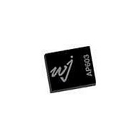
RF Modules & Development Tools 869-960MHz Eval Brd 17dB Gain

AP603-PCB900

Manufacturer Part Number
AP603-PCB900
Description
RF Modules & Development Tools 869-960MHz Eval Brd 17dB Gain
Manufacturer
TriQuint
Datasheet

Specifications of AP603-PCB900

Board Size
6 mm x 5 mm x 1 mm
Minimum Frequency
869 MHz
Minimum Operating Temperature
- 40 C
Supply Voltage (min)
28 V
Product
RF Development Tools
Maximum Frequency
960 MHz
Output Power
7 W
Supply Voltage (max)
80 V
Supply Current
246 mA
Maximum Operating Temperature
+ 85 C
For Use With/related Products
AP603
Lead Free Status / RoHS Status
Lead free / RoHS Compliant
Other names
1067337
WJ Communications, Inc • Phone 1-800-WJ1-4401 • FAX: 408-577-6621 • e-mail: sales@wj.com • Web site: www.wj.com, www.TriQuint.com
Product Features
Applications
Specifications
W-CDMA 3GPP Test Model 1+64 DPCH, 60% clipping, PAR = 8.6 dB
Absolute Maximum Rating
Operation of this device above any of these parameters may cause permanent damage.
Parameter
Operational Bandwidth
Test Frequency
Output Channel Power
Power Gain
Input Return Loss
Output Return Loss
ACLR
IMD3 @ +30 dBm PEP
PIN_VPD Current, Ipd
Operating Current, Icc
Collector Efficiency
Output P1dB
Quiescent Current, Icq
Vpd, Vbias
Vcc
Parameter
Storage Temperature, T
Junction Temperature, T
RF Input Power (CW tone), P
Breakdown Voltage C-B, BV
Breakdown Voltage C-E, BV
Quiescent Bias Current, I
Power Dissipation, P
@ 0.01% Probability, 3.84 MHz BW, Vcc = +28V, Icq = 160 mA
800 – 2200 MHz
+38.5 dBm P1dB
-50 dBc ACLR @ 1W P
-51 dBc IMD3 @ 1W PEP
15% Efficiency @ 1W P
Internal Active Bias
Internal Temp Compensation
Capable of handling 7:1 VSWR @
28 Vcc, 2.14 GHz, 5.5W CW Pout
Lead-free/RoHS-compliant
5x6 mm power DFN package
Mobile Infrastructure
High Power Amplifier (HPA)
For 10
6
hours MTTF
AP603
High Dynamic Range 7W 28V HBT Amplifier
DISS
stg
J
CQ
AVG
AVG
CEO
CBO
in
Units Min
MHz
MHz
dBm
dBm
dBc
dBc
mA
mA
mA
dB
dB
dB
%
V
V
Rating
-55 to +125 ºC
192 ºC
Input P6dB
80 V @ 0.1 mA
51 V @ 0.1 mA
320 mA
9.5 W
The AP603 is a high dynamic range power amplifier in a
lead-free/RoHS-compliant 5x6mm power DFN SMT
package. The single stage amplifier has excellent backoff
linearity, while being able to achieve high performance for
800-2200 MHz applications with up to +38.5 dBm of
compressed 1dB power.
The AP603 uses a high reliability, high voltage
InGaP/GaAs HBT process technology.
incorporates proprietary bias circuitry to compensate for
variations in linearity and current draw over temperature.
The module does not require any negative bias voltage; an
internal active bias allows the AP603 to operate directly off
a commonly used high voltage supply (typically +24 to
+32V). An added feature allows the quiescent bias to be
adjusted externally to meet specific system requirements.
The AP603 is targeted for use as a pre-driver and driver
stage amplifier in wireless infrastructure where high
linearity and high efficiency is required. This combination
makes the device an excellent candidate for next generation
multi-carrier 3G mobile infrastructure.
800
+38.2
Typ
2140
11.8
14.6
+30
+28
246
160
8.2
-50
-51
Product Description
10
+5
4
Max
2200
Typical Performance
W-CDMA 3GPP Test Model 1+64 DPCH, 60% clipping, PAR = 8.6 dB
Notes:
1. The reference designs shown in this datasheet have the device optimized for WCDMA ACLR
2. The AP603 evaluation board has been tested for ruggedness to be capable of handling:
Ordering Information
@ 0.01% Probability, 3.84 MHz BW, Vcc = +28V, Icq = 160 mA
Parameter
Test Frequency
Channel Power
Power Gain
Input Return Loss
Output Return Loss
ACLR
IMD3 @ +30 dBm PEP
Operating Current, Icc
Collector Efficiency
Output P1dB
Quiescent Current, Icq
Vpd, Vbias
Vcc
Part No.
AP603-F
AP603-PCB900
AP603-PCB1960 1930-1990 MHz Evaluation board
AP603-PCB2140 2110-2170 MHz Evaluation board
performance at +25° C. Biasing for the amplifier is suggested at Vcc = +28V and Icq = 160 mA to
achieve the best tradeoff in terms of efficiency and linearity. Increasing Icq will improve upon the
device linearity (IMD3 and ACLR), but will decrease the efficiency performance slightly. More
information is given in the other parts of this datasheet.
7:1 VSWR @ +28 Vcc, 2140 MHz, 5.5W CW Pout,
5:1 VSWR @ +30 Vcc, 2140 MHz, 5.5W CW Pout,
3:1 VSWR @ +32 Vcc, 2140 MHz, 5.5W CW Pout.
The device
Specifications and information are subject to change without notice
Description
High Dynamic Range 28V 7W HBT Amplifier
920-960 MHz Evaluation board
Functional Diagram
Units
MHz
-30
-40
-50
-60
-70
-80
dBm
dBm
dBc
dBc
mA
mA
dB
dB
dB
%
V
V
26
CW 2-tone signal, 2140 MHz, ∆f = 1 MHz, Vcc = 28V, 25 ˚C
28
IMD3 vs. Output Power vs. Icq
+38.5
Output Power, PEP (dBm)
16.6
940
+30
217
-52
-52
5.5
17
11
Page 1 of 14 May 2007 ver 1
30
Typical
+38.5
1960
15.5
+30
+28
230
160
7.5
-49
-52
32
13
13
+5
34
+38.2
2140
11.8
14.6
80 mA
160 mA
260 mA
+30
246
-50
-51
8.2
10
36

Related parts for AP603-PCB900

AP603-PCB900 Summary of contents

Page 1

... VSWR @ +32 Vcc, 2140 MHz, 5.5W CW Pout. Rating -55 to +125 ºC Ordering Information 192 ºC Part No. Input P6dB AP603 0.1 mA AP603-PCB900 0.1 mA AP603-PCB1960 1930-1990 MHz Evaluation board 320 mA AP603-PCB2140 2110-2170 MHz Evaluation board 9.5 W Functional Diagram The device IMD3 vs. Output Power vs. Icq CW 2-tone signal, 2140 MHz, ∆ ...

Page 2

... Device S-parameters are available for download off of the website at: http://www.wj.com Test condition: Output Power = 29.5 dBm, V Test signal = W-CDMA (PAR=8.6dB @ 0.01% Probability), 2140 MHz The reference plane is at the AP603-PCB2140 eval board’s SMA connectors. The plots are shown to detail the optimization of the ACLR performance. Gain Load-Pull GAIN Max=13. 76.9-j37.0 WJ Communications, Inc • ...

Page 3

... Vpd is used as a reference for the internal active bias circuitry. It can be used to turn on/off the amplifier. Ipd depends on the Icq quiescent current setting. Ipd can 8mA at a quiescent current setting of 320mA. 3. Vbias should be maintained fixed at +5V. Ibias will change based on RF input power level. It can 8mA on the AP603 ...

Page 4

... The center of C28 is placed at 0.220” (8.4° @ 880 MHz) from the edge of the AP603 (U1). 5. The center placed at 0.200” (7.7° @ 880 MHz) from the edge of the AP603 (U1). 6. The center of C31 is placed at 0.360” (13.8° @ 880 MHz) from the center of L4. ...

Page 5

... AP603 High Dynamic Range 7W 28V HBT Amplifier 920-960 MHz Application Circuit (AP603-PCB900) Typical WCDMA Performance at 25 ° channel power of +30 dBm Frequency 940 MHz W-CDMA Channel Power +30 dBm Power Gain 17 dB Input Return Loss 11 dB Output Return Loss 5.5 dB ACLR -52 dBc ...

Page 6

... The center placed at 0.100” (8.5° @ 1960 MHz) from the edge of the AP603 (U1). 5. The center of C28 is placed at 0.300” (25.6° @ 1960 MHz) from the edge of the AP603 (U1). 6. The center of C29 is placed at 0.420” (35.9° @ 1960 MHz) from the center of C28. ...

Page 7

... AP603 High Dynamic Range 7W 28V HBT Amplifier 1930-1990 MHz Application Circuit Performance Plots W-CDMA 3GPP Test Model 1+64 DPCH, 60% clipping, PAR = 8 0.01% Probability, 3.84 MHz BW Gain vs. Output Power vs. Vcc CW tone, Icq = 160 mA, 1960 MHz, 25 ˚ ACLR1 vs. Output Power vs. Vcc WCDMA, Icq = 160 mA, 1960 MHz, 25 ˚C ...

Page 8

... High Dynamic Range 7W 28V HBT Amplifier 1930-1990 MHz Application Note: Changing Icq Biasing Configurations The AP603 can be configured to be operated with lower bias current by varying the bias-adjust resistor – R2. The recommended circuit configurations shown previously in this datasheet have the device operating with a 160 mA as the quiescent current (I ) ...

Page 9

... The center placed at 0.125” (11.0° @ 2015 MHz) from the edge of the AP603 (U1). 7. The center of C30 is placed at 0.250” (41.2° @ 2015 MHz) from the edge of the AP603 (U1). 8. The center of C19 is placed at 0.490” (43.0° @ 2015 MHz) from the center of C23. ...

Page 10

... The center placed at 0.085” (7.9° @ 2140 MHz) from the edge of the AP603 (U1). 6. The center of C23 is placed at 0.245” (22.9° @ 2140 MHz) from the edge of the AP603 (U1). 7. The center of C19 is placed at 0.475” (44.3° @ 2140 MHz) from the center of C23. ...

Page 11

... AP603 High Dynamic Range 7W 28V HBT Amplifier 2110-2170 MHz Application Circuit Performance Plots W-CDMA 3GPP Test Model 1+64 DPCH, 60% clipping, PAR = 8 0.01% Probability, 3.84 MHz BW Gain vs. Output Power vs. Temperature CW tone, Vcc = 28V, Icq = 160 mA, 2140 MHz -40 ˚ ˚C 85 ˚ Output Power (dBm) AM-PM vs. Input Power 2140 MHz, Vcc = 28V, Icq = 160 mA, 25 ˚ ...

Page 12

... High Dynamic Range 7W 28V HBT Amplifier 2110-2170 MHz Application Note: Changing Icq Biasing Configurations The AP603 can be configured to be operated with lower bias current by varying the bias-adjust resistor – R2. The recommended circuit configurations shown previously in this datasheet have the device operating with a 160 mA as the quiescent current (I ) ...

Page 13

... The center placed at 0.070” (6.5° @ 2140 MHz) from the edge of the AP603 (U1). 6. The center of C28 is placed at 0.190” (17.7° @ 2140 MHz) from the edge of the AP603 (U1). 7. The center of C29 is placed at 0.300” (28.0° @ 2140 MHz) from the center of C28. ...

Page 14

... Junction Temperature (°C) Product Marking The component will be laser marked with an “AP603-F” product label with an alphanumeric lot code on the top surface of the package. Tape and reel specifications for this part will be located on the website in the “Application Notes” section. ...

Related keywords