EFM32G880F64 Energy Micro, EFM32G880F64 Datasheet
EFM32G880F64
Specifications of EFM32G880F64
Available stocks


Related parts for EFM32G880F64


EFM32G880F64 Summary of contents
Page 1
EFM32G880 DATASHEET F128/F64/F32 • ARM Cortex-M3 CPU platform • High Performance 32-bit processor @ MHz • Memory Protection Unit • Wake-up Interrupt Controller • Flexible Energy Management System • Shutoff Mode • ...
Page 2
... Ordering Information Table 1.1 (p. 2) shows the available EFM32G880 devices. Table 1.1. Ordering Information Ordering Code Flash (KB) EFM32G880F32-QFP100 32 EFM32G880F64-QFP100 64 EFM32G880F128-QFP100 128 Visit www.energymicro.com for information on global distributors and representatives or contact sales@energymicro.com for additional information. 1.1 Block Diagram A block diagram of the EFM32G880 is shown in Figure 1.1 ( ...
Page 3
System Summary 2.1 System Introduction The EFM32 MCUs are the world’s most energy friendly microcontrollers. With a unique combination of the powerful 32-bit ARM Cortex-M3, innovative low energy techniques, short wake-up time from energy saving modes, and a wide ...
Page 4
The high degree of flexibility enables software to minimize energy consumption in any specific application by not wasting power on peripherals and oscillators that are inactive. 2.1.8 Watchdog (WDOG) ...
Page 5
Low Energy Universal Asynchronous Receiver/Transmitter (LEUART) TM The unique LEUART , the Low Energy UART UART that allows two-way UART communication on a strict power budget. Only a 32.768 kHz clock is needed to allow UART communication ...
Page 6
Digital to Analog Converter (DAC) The Digital to Analog Converter (DAC) can convert a digital value to an analog output voltage. The DAC is fully differential rail-to-rail, with 12-bit resolution. It has two single ended output buffers which can ...
Page 7
Module PRS EBI I2C0 USART0 USART1 USART2 UART0 LEUART0 LEUART1 TIMER0 TIMER1 TIMER2 RTC LETIMER0 PCNT0 PCNT1 PCNT2 ACMP0 ACMP1 VCMP ADC0 DAC0 AES GPIO LCD 2.3 Memory Map The EFM32G880 memory map is shown in Figure 2.1 (p. 8) ...
Page 8
Figure 2.1. EFM32G880 Memory Map with largest RAM and Flash sizes 2010-12-17 - d0009_Rev1.20 ...the world's most energy friendly microcontrollers www.energymicro.com 8 ...
Page 9
Electrical Characteristics 3.1 Test Conditions 3.1.1 Typical Values The typical data are based on T lation and/or technology characterisation unless otherwise specified. 3.1.2 Minimum and Maximum Values The minimum and maximum values represent the worst conditions of ambient temperature, ...
Page 10
Environmental Table 3.3. Environmental Symbol Parameter V ESD (Human Body Model ESDHBM HBM) V ESD (Charged Device ESDCDM Model, CDM) Latch-up sensitivity test passed level A according to JEDEC JESD 78B method Class II, 85°C. 2010-12-17 - d0009_Rev1.20 ...the ...
Page 11
Current Consumption Table 3.4. Current Consumption Symbol Parameter EM0 current. No prescal- ing. Running prime num- I EM0 ber calculation code from Flash. I EM1 current EM1 I EM2 current EM2 I EM3 current EM3 I EM4 current EM4 ...
Page 12
Figure 3.1. EM0 Current consumption while executing prime number calculation code from flash with HFRCO running at 28MHz 5.3 5.2 5.1 5.0 4.9 4.8 4.7 4.6 2.0 2.2 2.4 2.6 2.8 3.0 Vdd [V] Figure 3.2. EM0 Current consumption while ...
Page 13
Figure 3.3. EM0 Current consumption while executing prime number calculation code from flash with HFRCO running at 14MHz 2.75 2.70 2.65 2.60 2.55 2.50 2.45 2.40 2.35 2.0 2.2 2.4 2.6 2.8 3.0 Vdd [V] Figure 3.4. EM0 Current consumption ...
Page 14
Figure 3.5. EM0 Current consumption while executing prime number calculation code from flash with HFRCO running at 7MHz 1.45 1.40 1.35 1.30 1.25 1.20 2.0 2.2 2.4 2.6 2.8 3.0 Vdd [V] Figure 3.6. EM1 Current consumption with all peripheral ...
Page 15
Figure 3.7. EM1 Current consumption with all peripheral clocks disabled and HFRCO running at 21MHz 1.08 1.06 1.04 1.02 1.00 0.98 0.96 0.94 0.92 2.0 2.2 2.4 2.6 2.8 3.0 Vdd [V] Figure 3.8. EM1 Current consumption with all peripheral ...
Page 16
Figure 3.9. EM1 Current consumption with all peripheral clocks disabled and HFRCO running at 11MHz 0.62 0.60 0.58 0.56 0.54 0.52 2.0 2.2 2.4 2.6 2.8 3.0 Vdd [V] Figure 3.10. EM1 Current consumption with all peripheral clocks disabled and ...
Page 17
Figure 3.11. EM2 current consumption. RTC prescaled to 1kHz, 32 kHz LFRCO. 3.5 3.0 2.5 2.0 1.5 1.0 0.5 1.8 2.0 2.2 2.4 2.6 2.8 3.0 Vdd [V] Figure 3.12. EM3 current consumption. 3.0 2.5 2.0 1.5 1.0 0.5 0.0 ...
Page 18
Figure 3.13. EM4 current consumption. 0.45 - 40.0°C - 15.0°C 0.40 5.0°C 25.0°C 45.0°C 0.35 65.0°C 85.0°C 0.30 0.25 0.20 0.15 0.10 0.05 0.00 1.8 2.0 2.2 2.4 2.6 2.8 3.0 Vdd [V] 3.5 Transition between Energy Modes Table 3.5. ...
Page 19
Table 3.6. Power Management Symbol Parameter V BOD threshold on falling BODextthr- external supply voltage V BOD threshold on falling BODintthr- internally regulated supply voltage V BOD threshold on rising ex- BODextthr+ ternal supply voltage t Delay from reset is ...
Page 20
General Purpose Input Output Table 3.8. GPIO Symbol Parameter V Input low voltage IOIL V Input high voltage IOIH V Output high voltage IOOH V Output low voltage IOOL I Input leakage current IOLEAK R I/O pin pull-up resistor ...
Page 21
Figure 3.14. Typical Low-Level Output Current, 2V Supply Voltage 0.20 0.15 0.10 0.05 0.00 0.0 0.5 1.0 Low- Level Output Voltage [V] GPIO_Px_CTRL DRIVEMODE = LOWEST 0.0 0.5 1.0 Low- Level Output Voltage [V] GPIO_Px_CTRL ...
Page 22
Figure 3.15. Typical High-Level Output Current, 2V Supply Voltage 0.00 - 40°C 25°C 85°C –0.05 –0.10 –0.15 –0.20 0.0 0.5 1.0 High- Level Output Voltage [V] GPIO_Px_CTRL DRIVEMODE = LOWEST 0 - 40°C 25°C 85°C –5 –10 –15 –20 0.0 ...
Page 23
Figure 3.16. Typical Low-Level Output Current, 3V Supply Voltage 0.5 0.4 0.3 0.2 0.1 0.0 0.0 0.5 1.0 1.5 Low- Level Output Voltage [V] GPIO_Px_CTRL DRIVEMODE = LOWEST 0.0 0.5 1.0 ...
Page 24
Figure 3.17. Typical High-Level Output Current, 3V Supply Voltage 0.0 - 40°C 25°C 85°C –0.1 –0.2 –0.3 –0.4 –0.5 0.0 0.5 1.0 1.5 High- Level Output Voltage [V] GPIO_Px_CTRL DRIVEMODE = LOWEST 0 - 40°C 25°C 85°C –10 –20 –30 ...
Page 25
Figure 3.18. Typical Low-Level Output Current, 3.8V Supply Voltage 0.8 0.7 0.6 0.5 0.4 0.3 0.2 0.1 0.0 0.0 0.5 1.0 1.5 2.0 Low- Level Output Voltage [V] GPIO_Px_CTRL DRIVEMODE = LOWEST 0.0 0.5 ...
Page 26
Figure 3.19. Typical High-Level Output Current, 3.8V Supply Voltage 0.0 - 40°C 25°C 85°C –0.1 –0.2 –0.3 –0.4 –0.5 –0.6 –0.7 –0.8 0.0 0.5 1.0 1.5 2.0 High- Level Output Voltage [V] GPIO_Px_CTRL DRIVEMODE = LOWEST 0 - 40°C 25°C ...
Page 27
Oscillators 3.9.1 LFXO Table 3.9. LFXO Symbol Parameter f Supported nominal crystal LFXO frequency ESR Supported crystal equiv- LFXO alent series resistance (ESR) C Supported crystal external LFXOL load range DC Duty cycle LFXO I Current consumption for LFXO ...
Page 28
LFRCO Table 3.11. LFRCO Symbol Parameter f Oscillation frequency , LFRCO =25°C DD AMB t Startup time not including LFRCO software calibration I Current consumption LFRCO TC Temperature coefficient LFRCO VC Supply voltage coefficient ...
Page 29
HFRCO Table 3.12. HFRCO Symbol Parameter Oscillation frequency HFRCO 3 =25°C AMB t Settling time after start-up HFRCO_settling I Current consumption HFRCO DC Duty cycle HFRCO Temperature coefficient, TC HFRCO ...
Page 30
Figure 3.21. Calibrated HFRCO 1 MHz Band Frequency vs Temperature and Supply Voltage 1.30 1.25 1.20 1.15 1.10 1.05 1.00 0.95 0.90 0.85 1.8 2.2 2.6 3.0 Vdd [V] Figure 3.22. Calibrated HFRCO 7 MHz Band Frequency vs Temperature and ...
Page 31
Figure 3.24. Calibrated HFRCO 14 MHz Band Frequency vs Temperature and Supply Voltage 14.15 14.10 14.05 14.00 13.95 13.90 13.85 1.8 2.2 2.6 3.0 Vdd [V] Figure 3.25. Calibrated HFRCO 21 MHz Band Frequency vs Temperature and Supply Voltage 21.2 ...
Page 32
ULFRCO Table 3.13. ULFRCO Symbol Parameter f Oscillation frequency ULFRCO TC Temperature coefficient ULFRCO VC Supply voltage coefficient ULFRCO 3.10 Analog Digital Converter (ADC) Table 3.14. ADC Symbol Parameter V Input voltage range ADCIN V Input range of external ...
Page 33
Symbol Parameter C Input RC filter/decoupling ADCFILT capacitance f ADC Clock Frequency ADCCLK t Conversion time ADCCONV t Acquisition time ADCACQ t Required acquisition time ADCACQVDD3 for VDD/3 reference Startup time of reference generator and ADC core in NORMAL mode ...
Page 34
Symbol Parameter Signal to Noise-puls-Distor- SNDR ADC tion Ratio (SNDR) 2010-12-17 - d0009_Rev1.20 ...the world's most energy friendly microcontrollers Condition Min 200 kSamples/s, 12 bit, dif- ferential, internal 1.25V refer- ence 200 kSamples/s, 12 bit, differ- ential, internal 2.5V reference ...
Page 35
Symbol Parameter Spurious-Free Dynamic SFDR ADC Range (SFDR) V Offset voltage ADCOFFSET Thermometer output gradi- TGRAD ADCTH ent DNL Differential non-linearity ADC (DNL) INL Integral non-linearity (INL), ADC End point method 2010-12-17 - d0009_Rev1.20 ...the world's most energy friendly microcontrollers ...
Page 36
Symbol Parameter MC No missing codes ADC 1 On the average every ADC will have one missing code, most likely to appear around 2048 +/- n*512 where n can be a value in the set {-3, -2, - ...
Page 37
Typical performance Figure 3.29. ADC Frequency Spectrum, Vdd = 3V, Temp = 25° 0 –20 –40 –60 –80 –100 –120 –140 –160 –180 Frequency [kHz] 1.25V Reference 0 –20 –40 –60 –80 –100 –120 –140 ...
Page 38
Figure 3.30. ADC Integral Linearity Error vs Code, Vdd = 3V, Temp = 25° 1.5 1.0 0.5 0.0 –0.5 –1.0 0 512 1024 1536 2048 2560 Output code 1.25V Reference 0.8 0.6 0.4 0.2 0.0 –0.2 –0.4 –0.6 0 512 ...
Page 39
Figure 3.31. ADC Differental Linearity Error vs Code, Vdd = 3V, Temp = 25° 1.0 0.5 0.0 –0.5 –1.0 0 512 1024 1536 2048 2560 Output code 1.25V Reference 1.0 0.5 0.0 –0.5 –1.0 0 512 1024 1536 2048 2560 ...
Page 40
Figure 3.32. ADC Absolute Offset, Common Mode = Vdd / –1 –2 –3 –4 2.0 2.2 2.4 2.6 2.8 3.0 Vdd (V) Offset vs Supply Voltage, Temp = 25° Figure 3.33. ADC Dynamic Performance ...
Page 41
Figure 3.34. ADC Temperature sensor readout 2600 2500 2400 2300 2200 2100 –40 –25 –15 – Tem perature [°C] 3.11 Digital Analog Converter (DAC) Table 3.15. DAC Symbol Parameter V Output voltage range DACOUT V Output ...
Page 42
Symbol Parameter Signal to Noise-pulse Dis- SNDR DAC tortion Ratio (SNDR) Spurious-Free Dynamic SFDR DAC Range(SFDR) V Offset voltage DACOFFSET V Sample-hold mode voltage DACSHMDRIFT drift DNL Differential non-linearity DAC INL Integral non-linearity DAC MC No missing codes DAC 2010-12-17 ...
Page 43
Analog Comparator (ACMP) Table 3.16. ACMP Symbol Parameter V Input voltage range ACMPIN V ACMP Common Mode volt- ACMPCM age range I Active current ACMP Current consumption of in- I ACMPREF ternal voltage reference V Offset voltage ACMPOFFSET V ...
Page 44
Figure 3.35. Typical ACMP Characteristics 2.5 2.0 1.5 1.0 0.5 0 ACMP_CTRL_BIASPROG Current consumption 100 BIASPROG= 0.0 BIASPROG= 4.0 BIASPROG= 8.0 BIASPROG= 12 ACMP_CTRL_HYSTSEL Hysteresis 2010-12-17 - d0009_Rev1.20 ...
Page 45
Voltage Comparator (VCMP) Table 3.17. VCMP Symbol Parameter V Input voltage range VCMPIN V VCMP Common Mode volt- VCMPCM age range I Active current VCMP t Startup time reference gen- VCMPREF erator V Offset voltage VCMPOFFSET V VCMP hysteresis ...
Page 46
LCD Table 3.18. LCD Symbol Parameter f Frame rate LCDFR NUM Number of segments sup- SEG ported V LCD supply voltage range LCD Steady state current con- I LCD sumption. Steady state Current contri- I LCDBOOST bution of internal ...
Page 47
Symbol Parameter I LEUART current LEUART I I2C current I2C I TIMER current TIMER I LETIMER current LETIMER I PCNT current PCNT I RTC current RTC I LCD current LCD I AES current AES I GPIO current GPIO I EBI ...
Page 48
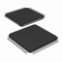
Pinout and Package Note Please refer to the application note "AN0002 EFM32 Hardware Design Considerations" for guidelines on designing Printed Circuit Boards (PCB's) for the EFM32G880. 4.1 Pinout The EFM32G880 pinout is shown in Figure 4.1 (p. 48) and ...
Page 49
LQFP100 Pin# and Name Pin Analog Name 4 PA3 LCD_SEG16 5 PA4 LCD_SEG17 6 PA5 LCD_SEG18 7 PA6 LCD_SEG19 8 IOVDD_0 Digital IO power supply 0. 9 PB0 LCD_SEG32 10 PB1 LCD_SEG33 11 PB2 LCD_SEG34 12 PB3 LCD_SEG20 13 PB4 ...
Page 50
LQFP100 Pin# and Name Pin Analog Name 41 AVDD_1 Analog power supply PB13 HFXTAL_P #0 43 PB14 HFXTAL_N #0 44 IOVDD_3 Digital IO power supply 3. 45 AVDD_0 Analog power supply 0. 46 PD0 ADC0_CH0 #0 47 ...
Page 51
LQFP100 Pin# and Name Pin Analog Name 76 PF0 77 PF1 78 PF2 LCD_SEG0 79 PF3 LCD_SEG1 80 PF4 LCD_SEG2 81 PF5 LCD_SEG3 82 IOVDD_5 Digital IO power supply 5. 83 VSS Ground 84 PF6 LCD_SEG24 85 PF7 LCD_SEG25 86 ...
Page 52
Alternate LOCATION Functionality 0 1 ACMP0_CH1 PC1 ACMP0_CH2 PC2 ACMP0_CH3 PC3 ACMP0_CH4 PC4 ACMP0_CH5 PC5 ACMP0_CH6 PC6 ACMP0_CH7 PC7 ACMP0_O PE13 PE2 ACMP1_CH0 PC8 ACMP1_CH1 PC9 ACMP1_CH2 PC10 ACMP1_CH3 PC11 ACMP1_CH4 PC12 ACMP1_CH5 PC13 ACMP1_CH6 PC14 ACMP1_CH7 PC15 ACMP1_O PF2 ...
Page 53
Alternate LOCATION Functionality 0 1 EBI_AD06 PE14 EBI_AD07 PE15 EBI_AD08 PA15 EBI_AD09 PA0 EBI_AD10 PA1 EBI_AD11 PA2 EBI_AD12 PA3 EBI_AD13 PA4 EBI_AD14 PA5 EBI_AD15 PA6 EBI_ALE PF3 EBI_ARDY PF2 EBI_CS0 PD9 EBI_CS1 PD10 EBI_CS2 PD11 EBI_CS3 PD12 EBI_REn PF5 EBI_WEn ...
Page 54
Alternate LOCATION Functionality 0 1 LCD_SEG7 PE11 LCD_SEG8 PE12 LCD_SEG9 PE13 LCD_SEG10 PE14 LCD_SEG11 PE15 LCD_SEG12 PA15 LCD_SEG13 PA0 LCD_SEG14 PA1 LCD_SEG15 PA2 LCD_SEG16 PA3 LCD_SEG17 PA4 LCD_SEG18 PA5 LCD_SEG19 PA6 LCD_SEG20 PB3 LCD_SEG21 PB4 LCD_SEG22 PB5 LCD_SEG23 PB6 LCD_SEG24 ...
Page 55
Alternate LOCATION Functionality 0 1 LFXTAL_P PB7 PCNT0_S0IN PC13 PE0 PCNT0_S1IN PC14 PE1 PCNT1_S0IN PC4 PB3 PCNT1_S1IN PC5 PB4 PCNT2_S0IN PD0 PE8 PCNT2_S1IN PD1 PE9 TIM0_CC0 PA0 PA0 TIM0_CC1 PA1 PA1 TIM0_CC2 PA2 PA2 TIM0_CDTI0 PA3 PC13 TIM0_CDTI1 PA4 PC14 ...
Page 56
GPIO pinout overview The specific GPIO pins available in EFM32G880 is shown in Table 4.3 (p. 56) . Each GPIO port is organized as 16-bit ports indicated by letters A through F, and the individual pin on this port ...
Page 57
These dimensions apply to the flat section between 0.10 mm and 0.25 mm from the lead tip. 6. 'A1' is defined as the distance from the seating plan to the lowest point on the package body. 7. Package dimensions ...
Page 58
PCB Layout and Soldering 5.1 Recommended PCB Layout Figure 5.1. LQFP100 PCB Land Pattern 1.45 0.30 0.50 Figure 5.2. LQFP100 PCB Solder Mask 1.57 0.42 0.50 2010-12-17 - d0009_Rev1.20 ...the world's most energy friendly microcontrollers 100 ...
Page 59
Figure 5.3. LQFP100 PCB Stencil Design 1.35 0.20 0.50 1. The drawings are not to scale. 2. All dimensions are in millimeters. 3. All drawings are subject to change without notice. 4. The PCB Land Pattern drawing is in compliance ...
Page 60
Chip Marking, Revision and Errata 6.1 Chip Marking In the illustration below package fields and position are shown. Figure 6.1. Example Chip Marking 6.2 Revision The revision of a chip can be determined from the "Revision" field in Figure ...
Page 61
Revision History 7.1 Revision 1.20 December 17th, 2010 Increased max storage temperature. Added data for <150°C and <70°C on Flash data retention. Changed latch-up sensitivity test description. Added IO leakage current Updated ESD CDM value. Added Flash current consumption ...
Page 62
Updated VCMP characterization data. 7.4 Revision 1.00 April 23rd, 2010 ADC_VCM line removed. Added pinout illustration and additional pinout table. Changed "Errata" chapter. Errata description moved to separate document. Document changed status from "Preliminary". Updated "Electrical Characteristics" chapter. 7.5 Revision ...
Page 63
Current consumption of digital peripherals added in Section 3.15 (p. 46) . Package information in Section 4.4 (p. 56) corrected. Updated errata section. 7.9 Revision 0.80 Initial preliminary revision, October 19th, 2009 2010-12-17 - d0009_Rev1.20 ...the world's most energy friendly ...
Page 64
... Micro reserves the right to make changes without further notice and limitation to product information, specifications, and descriptions herein, and does not give warranties as to the accuracy or completeness of the included information. Energy Micro shall have no liability for the consequences of use of the infor- mation supplied herein. This document does not imply or express copyright licenses granted hereunder to design or fabricate any integrated circuits. The products must not be used within any Life Support System without the specific written consent of Energy Micro. A " ...
Page 65
... B Contact Information B.1 Energy Micro Corporate Headquarters Postal Address Energy Micro AS P.O. Box 4633 Nydalen N-0405 Oslo NORWAY www.energymicro.com Phone: + Fax B.2 Global Contacts Visit www.energymicro.com for information on global distributors and representatives or contact sales@energymicro.com for additional information. Americas www.energymicro.com/americas www.energymicro.com/emea 2010-12-17 - d0009_Rev1.20 ...
Page 66
... Revision 0.83 ............................................................................................................................... 62 7.7. Revision 0.82 ............................................................................................................................... 62 7.8. Revision 0.81 ............................................................................................................................... 62 7.9. Revision 0.80 ............................................................................................................................... 63 A. Disclaimer and Trademarks ....................................................................................................................... 64 A.1. Disclaimer ................................................................................................................................... 64 A.2. Trademark Information ................................................................................................................... 64 B. Contact Information ................................................................................................................................. 65 B.1. Energy Micro Corporate Headquarters .............................................................................................. 65 B.2. Global Contacts ............................................................................................................................ 65 2010-12-17 - d0009_Rev1.20 ...the world's most energy friendly microcontrollers www.energymicro.com 66 ...
Page 67
List of Figures 1.1. Block Diagram ....................................................................................................................................... 2 2.1. EFM32G880 Memory Map with largest RAM and Flash sizes .......................................................................... 8 3.1. EM0 Current consumption while executing prime number calculation code from flash with HFRCO running at 28MHz ..................................................................................................................................................... 12 3.2. ...
Page 68
List of Tables 1.1. Ordering Information ................................................................................................................................ 2 2.1. Configuration Summary ............................................................................................................................ 6 3.1. Absolute Maximum Ratings ...................................................................................................................... 9 3.2. General Operating Conditions ................................................................................................................... 9 3.3. Environmental ....................................................................................................................................... 10 3.4. Current Consumption ............................................................................................................................. 11 3.5. Energy Modes Transitions ...................................................................................................................... 18 ...
Page 69
List of Equations 3.1. Total ACMP Active Current ..................................................................................................................... 43 3.2. VCMP Trigger Level as a Function of Level Setting ..................................................................................... 45 3.3. Total LCD Current Based on Operational Mode and Internal Boost ................................................................. 46 2010-12-17 - d0009_Rev1.20 ...the world's ...
Page 70
...