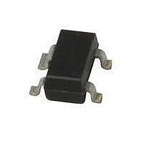
BF1105,215 NXP Semiconductors, BF1105,215 Datasheet - Page 8

BF1105,215
Manufacturer Part Number
BF1105,215
Description
MOSFET N-CH 7V DUAL SOT143
Manufacturer
NXP Semiconductors
Datasheet
1.BF1105R215.pdf
(15 pages)
Specifications of BF1105,215
Package / Case
SOT-143, SOT-143B, TO-253AA
Current Rating
30mA
Frequency
800MHz
Gain
38dB
Transistor Type
N-Channel Dual Gate
Noise Figure
1.7dB
Voltage - Test
5V
Configuration
Dual
Transistor Polarity
Dual N-Channel
Drain-source Breakdown Voltage
7 V
Continuous Drain Current
30 mA
Power Dissipation
200 mW
Mounting Style
SMD/SMT
Lead Free Status / RoHS Status
Lead free / RoHS Compliant
Power - Output
-
Current - Test
-
Lead Free Status / RoHS Status
Lead free / RoHS Compliant, Lead free / RoHS Compliant
NXP Semiconductors
1997 Dec 02
handbook, full pagewidth
handbook, full pagewidth
N-channel dual-gate MOS-FETs
V
L1 = 45 nH, 4 turns, internal diameter = 4 mm, 0.8 mm copper wire.
L2 = 160 nH, 3 turns, internal diameter = 8 mm, 0.8 mm copper wire; tapped at approximately half a turn from the cold side, to set G
C1 adjusted for G
V
L1 = 2 cm, silvered 0.8 mm copper wire 4 mm above ground plane.
L2 = 2 cm, silvered 0.8 mm copper wire 4 mm above ground plane.
L3 = 11 turns 0.5 mm copper wire without spacing, internal diameter = 3 mm, L = approx. 200 nH.
DS
DS
= 5 V, G
= 5 V, G
S
S
= 2 mS, G
= 3.3 mS, G
S
= 2 mS.
L
input
50 Ω
= 0.5 mS, f = 200 MHz.
L
= 1 mS, f = 800 MHz.
input
50 Ω
1 nF
5.5 pF
C1
2 to 18 pF
1 nF
L1
L1
1 nF
1 nF
1 nF
15
pF
V AGC
V AGC
Fig.16 Gain test circuit.
Fig.17 Gain test circuit.
0.5 to 3.5 pF
47 kΩ
1 nF
47 kΩ
BB405
G2
G1
G2
G1
V tun input
BF1105WR
BF1105R
BF1105WR
BF1105
BF1105R
BF1105
330 kΩ
8
1 nF
D
S
S
D
1 nF
1 nF
BF1105; BF1105R; BF1105WR
L2
V DS
0.5 to 3.5 pF
2 μH
BB405
10 pF
1 nF
L2
V tun output
V DS
output
330 kΩ
50 Ω
1 nF
L3
4 to 40 pF
1 nF
1 nF
MGM255
MGM256
output
50 Ω
Product specification
L
= 0.5 mS.


